Oh Say Can You C? – Grappling with the USB type-C Connector
USB - Universal Serial Bus. Let’s break that down.
- Universal. It works everywhere and for everyone.
- Serial. We’re cramming extra data into the stream relative to parallel busses.
- Bus. A bunch of wires.
So we have a bunch of wires with a bunch of data doing a bunch of things. It is a neat trick if you can pull it off. USB has been around for awhile and is most recognized as the connector format for the thumb drives, of which you probably have a few - or many if you get out to the trade shows and pick up the freebies. Your phone may have the micro-version, or it may have the even more micro USB type-C connector.
The wondrous thing about these gizmos is their ability to multitask. It is a charge port. It is a data port. It is a display port. It slices. It dices. But wait, there is more! There is no penalty for plugging it in upside down because it is not polarized like all of its predecessors.
I can honestly say that I was working on the USB-C protocol before USB-C was cool. Google was/is part of the specification development consortium. My first encounter was in early 2015 trying to create the little piece of circuitry between the wire and the plug. This bit is shrouded inside the charger assembly side of the equation. The board connectors came right after that little piece.
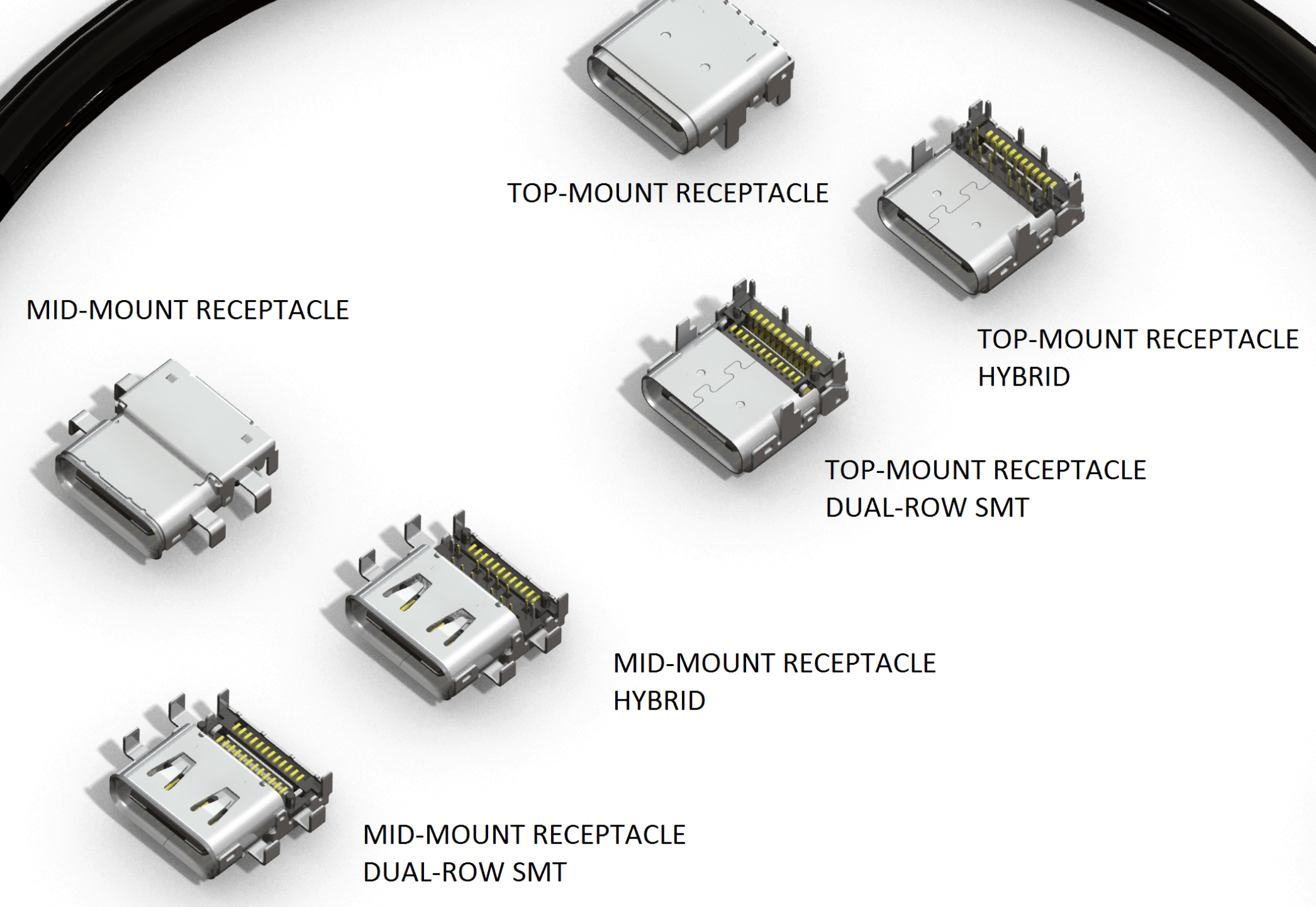
Most of you will be interested in that half of the connector pair because that is the part that goes on the printed circuit board. If you have not used the C connector in a design, you may be in for a few surprises. For one thing, it goes well beyond the simplicity of the traditional USB port.
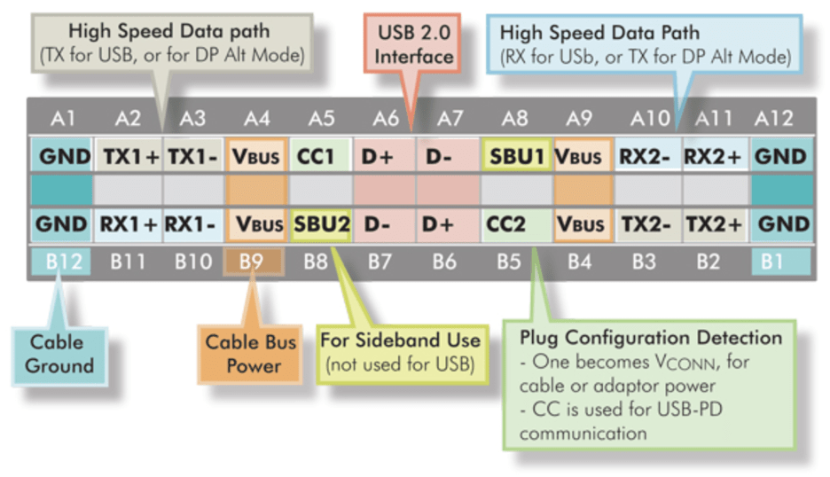
Image credit: Diodes.com
Even the most advanced PCB fabricators will struggle with the implementation. There may be exceptions, but I have yet to find a connector vendor who can pull off all of the requirements with a footprint that is within the fab shops’ manufacturing sweet spot. Most of us will plug our phone, tablet or computer in every night or more often for power users. That is a lot of engagements and a lot of chances to tug on the connector. I'm glad that the machine I'm using to write this is bristling with four USB-C connector ports. It's all but certain that there is a finite number of times that I can yank that cord before I wreck the pins on one side of the other.
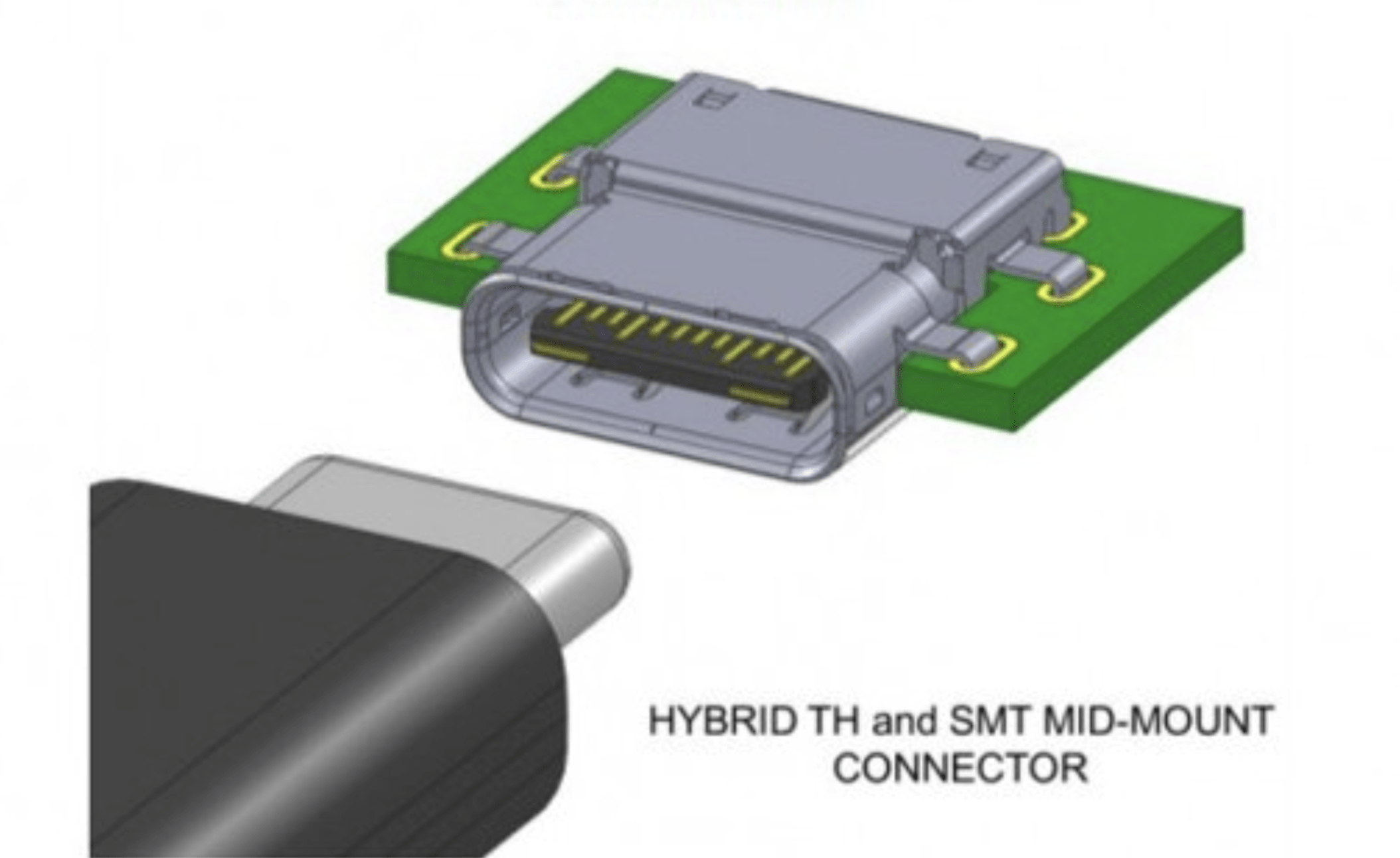 Image credit: Geek.com and several others
Knowing this, the connector vendors will specify a highly constrained footprint geometry. Expect a very tight location and size tolerance on a non-plated hole and a non-plated slot. Those are secondary drills that come after the first drill and route patterns used for the plated holes and slots. The plated slots for the body of the connector are often pushed right to the edge of the board. The surface mount pads are right up against the non-plated holes. If we're concerned about the Z-height of the entire device–and who isn't these days–we are compelled to use a mid-mount connector that rests in a slot in the PC Board. That little wrinkle adds through-hole for one row of leads while keeping one row of surface mount pads. Thus we have non-plated holes and slots along with plated holes in slots all in very close proximity to each other.
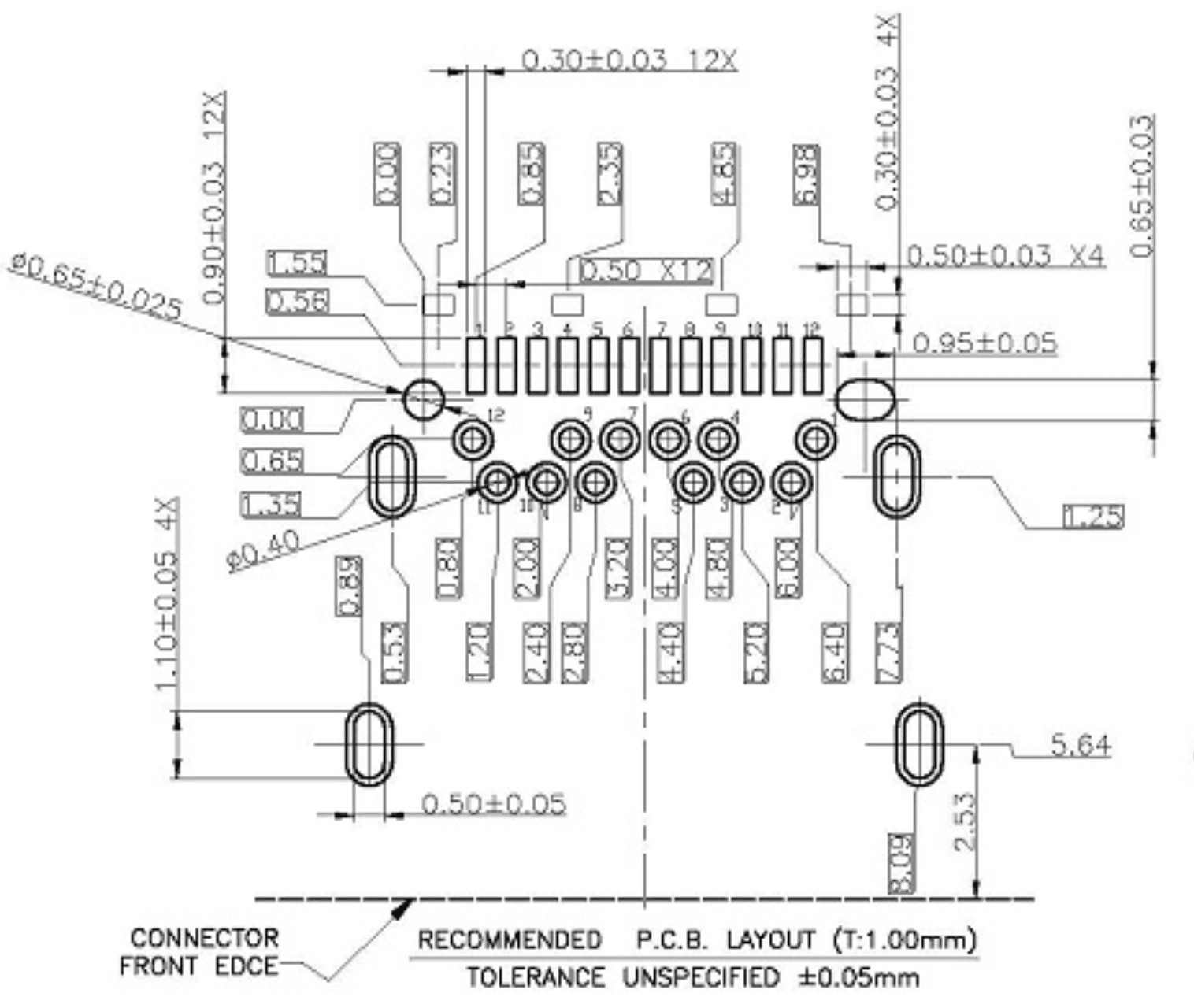
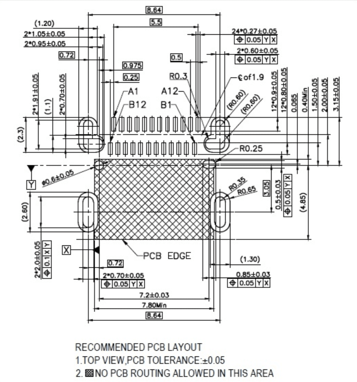
Image Credit: Datasheets from Witarea (mid-mount) and China Connector (SMD)
Recall that when we have a tooling hole, the metal pullback is always greater than the pull-back for plated holes. The process flow is drill, plate, drill. After those steps, the panel is put into a fixture for the non-plated holes. It may not be the same operator or the same location within the factory which can lead to a natural variation and is the reason for the larger keep-out area around the non-plated holes. Following the vendor's conservative footprint will inevitably lead to getting a DFM request from the fabricator.
- “Can we increase the tolerance of the non-plated hole/slot?”
- “Can we clip the pad of the plated slot at the edge of the board?”
- “Can we trim the SMD pad away from the non-plated hole?”
- “Can we move or delete those slots?”
Seriously? I've had these questions from fabricators who are at the top of the technology heap. Even outfits that can reliably etch 40 microns (!) trace and space struggle with the footprint of the USB-C connectors.
I was at DesignCon last year and visited several connector vendors; Amphenol, Lotes, Samtek, TE, and others. At the Lotes booth, they had a circular board about eight inches in diameter with different versions of USB-C connectors all the way around. I was only half joking with the rep when I told her that she should take her datasheets to every PCB Fabricator on the show floor and ask them to do a DFM study on their recommended footprint geometry. It's that much of a challenge.
There must have been others like me. Four years and counting, we’ve brought the connector vendor to the table on behalf of the fab-house -and our profit potential. New products are entering the market with their plated slots and pins pulled in from the edge. That breathing room allows us to fan-out with standard drilling operations. You can find the non-plated slot/hole pair away from the connect pins. That also helps the fabricator while providing another routing advantage. Here is a story of why that matters.
How Flexible are You?
Tolerances are that much harder to achieve in flex circuits so, of course, there was blowback when we put a C-connector on a six-layer flex circuit. With the isolation of the superspeed diff pairs and the gnarly power requirements of the laptop, it was not a very flexible flex. In fact, the device failed the three-foot drop onto concrete test as the special zero-insertion-force (ZIF) flex connector didn't have enough grip on the edge connector. My physical designer quickly fashioned a little bracket that cantilevered out from one side. I cleared away the traces, and it was game-on. As the Mythbusters would say as they put the crash test dummy on a chairlift with a laptop and an impact-fused stick of dynamite on his lap, “don't try this at home!”
The flex vendor predictably balked at the tight constraints and wanted spec relief and gang openings for the solder mask. I loved the response from our physical designer. He told the vendor that they were doing fabrication and assembly, (common on flexes) and that they alone would be responsible for all failures relating to this item. It is this liability, in my estimation, that has the connector vendors wanting a perfect starting footprint. They are not going to own the problem if you do not follow their design criteria.
What action you should take when the part vendors' requirements exceed the capability of the fab or assembly vendor became a standard interview question from that point forward. The answer is obvious. Bring them both to the table and try to find an acceptable middle ground.
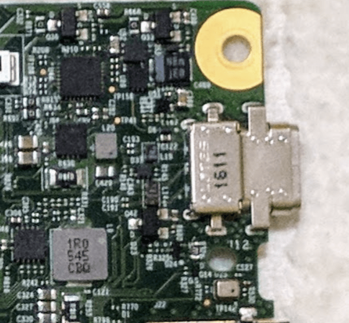
Photo: USB Type-C, top mounted
Getting Down to the Routing
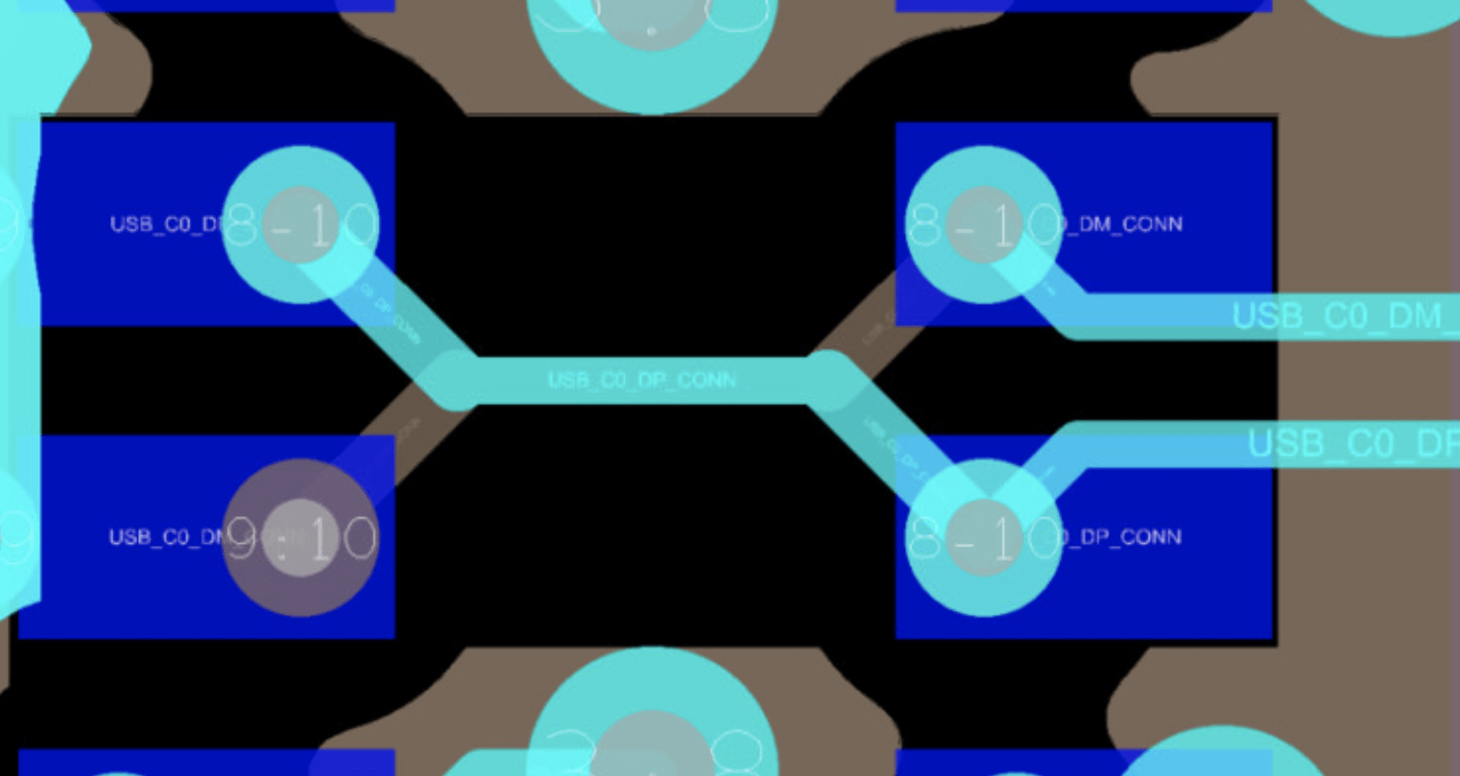
Ok, so now you have a USB-C connector footprint that can be produced by at least one company. You've got all of your ESD protection diodes right there by the connector to save the rest of the delicate devices. It's routing time. The first thing you might notice is that there is a differential pair of traces right down the middle of the connector that connects from the back row to the front row whether they are SMD or through-hole. This quartet of pins represent the legacy USB 2.0 interface. Remember that the mating connector will have to work right-side-up or upside-down as there is no polarity difference. What you get is a very short diff pair that crosses over P and N before leading out the ESD suppression circuits.
We can usually uncross a diff pair by diving into the board with vias and then start routing away on another layer in the same direction we entered rather than in a linear path. That's a trick that's harder to pull off in the limited space around this type of connector. I went back to an old analog trick. Standard couplers that you'd print on the PCB are made up of four ports that represent the In, Out, Terminated and Coupled signals in an analog design. The input port is a direct DC connection to the terminated port that goes to a resistor that is grounded on the other pin. The length that the two lines run along with the gap between them will establish the amount of coupling, 3dB, 10 and 20 dB are common. The coupled port and out port get their energy as that line is routed side by side with the other line.
On the other hand, a quadrature hybrid coupler runs the two lines on adjacent layers and the terminated port ends up on the opposite side rather than the same side as the input, forming an X, except the crossing is elongated to achieve the coupling. You see where this is going.
Back to the USB- C; run the two lines out of the central through pins or vias as the case may be on different layers, and create a broadside coupled pair rather than an edge coupled pair so you can cross over. I've shown this diagram before because I think it's the best solution to this routing plan. I used layers 8 and 9 in this case and micro-via-in-pad. Note that I switched to broadside coupled lines out to the ESD diodes.
Screenshot: USB 2.0 section
We want to minimize the length since you would either engage the inboard or outboard row of pads depending on how you plug in the mating connector. We live with the stub. Signal wise, this is the backward compatible part of the circuit so it’s not really that bad.
We’ve covered four pins; twenty to go. The next four that can be a challenge are the power pins. VBUS or VBAT are common names. This image from TI shows them in blue. We could be pulling 3 amps through those two vias. Three vias on each pair of pins would be preferable. Through hole solutions will not be quite so elegant as so much is going on in a constrained area.
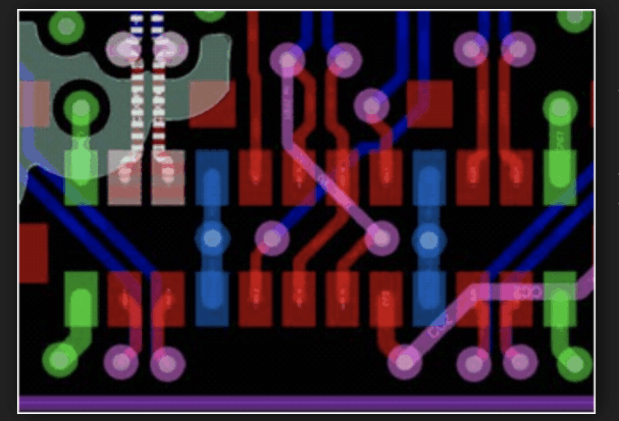
Image credit: TI
Between the USB2.0 section and the power pins, we have four housekeeping signals. While they look related, they’re not routed as pairs. I can recall being asked for additional width on some of them. Be prepared.
Four more diff-pairs are located between the power pins and the outboard ground pins. The diff-pairs have some areas that could be a squeeze play but the routing is otherwise straightforward. You will probably be looking at some other P and N entanglements between the device and the connector. Your normal bag of tricks should allow you to flip the bits as required. These may have the letters SS in the net-name. Super Speed routing needs your utmost care as far as good impedance practices.
The upshot here is that the USB type-C connector can be a beast to implement at the fab house and a challenging puzzle to fan-out. The benefit is that it is the all-in-one solution to power and data. This technology will be with us as long as 10 Gb per second still means something. Jump in a C what you can C.
References:
- https://www.wit-area.com/USB-C-Connector/USB31-TYPE-C-24P-DIPSMT-receptacleCH168mmL987mm48v-5A-240W/
- https://www.geek.com/chips/reversible-usb-type-c-connector-finalized-at-last-1601919/
- https://www.diodes.com/design/support/technical-articles/pericoms-articles/usb-type-c-is-coming-3-things-youve-just-gotta-know/
- http://www.ti.com/product/HD3SS460/datasheet/layout#SLLSEM76500