The Nuts and Bolts of a Via Padstack
The humble via comes in many flavors. By connecting one layer of a conductor pattern to another, vias have connected the world. My whole career has depended on them as part of the hardware I used to design for everyone else to use. A foundational innovation in electronics brought plated through holes to the masses. As a leap forward from wire-wrap technology, multi-layer printed circuit boards put a “mainframe” in each of our pockets almost overnight.
From the first plated through-hole to the latest, the trend is to support higher density interconnect. The key driver in plating holes is the aspect ratio, the hole’s width over depth. For a through-hole, the depth is the thickness of the PCB. Most reputable fab houses can handle a 10 to 1 ratio such that a popular .062” board thickness will require a minimum finished hole size 0.006”
Finished hole size is just what it says on the tin. The initial drill will be one or two-thousandths of an inch larger than the finished size to account for the thickness in the copper “barrel”. The barrel is created by drilling the through holes and electroplating the top and bottom of the board prior to etching away the circuit pattern. So there are these two complete sheets of copper of a starting thickness. As those are plated up, the prepared holes get their plating. That is all of the copper that is added to form the barrel. Other protective layers come later.

Image Credit: Author - 10 layers of technology.
Via Plating Thickness and the Effect of Trace Width, Air Gap and Other Factors
The point is that the optimum amount of barrel wall thickness is dependent on the outer-layer geometry of the PCB. Trace width and (especially) air-gap are heavily dependent on the thickness of the copper on the outer layers. You’ll note that most of the time, there is a different set of rules for inner vs. outer layers in terms of trace width and space. Up to a point, a larger hole will be easier to plate. As the smaller holes approach the maximum aspect ratio the plating has to be more aggressive. Pressing on the factory capabilities inevitably leads to more X-outs. As yield drops, unit prices rise.
If the density of the board permits, a 0.013” hole with a 0.25” capture pad is the sweet spot for low-cost PCBs. This would have good current capacity but could be too much a discontinuity for a high-speed link. In that case, a 0.008” finished hole through a 0.018” pad would be a good compromise and a go-to size for most plated through-hole designs. While inches were used, expect the metric system to apply for the most part.
With a solid via plan, one of the factors the user can influence is what to do when a via is not connected on a layer. I’ve been told that having a plated pad on the no-connect layer could expose the signal to magnetic coupling when the vias share an opening in the ground plane. I’ve also been told that the extra annular ring helps anchor the via’s barrel. That little extra copper that became the barrel could use those the same way a 55-gallon barrel has ridges. I use gallons because “208.198 liters”?

Image Credit: GlobalIndustrial
Live a little. When a layout can afford to spread out on the top layer, it is a chance to get to a useful routing grid. Take into account the number of channels that will route between each via. While it is tempting to pair each via to the SMD pad, optimizing the fan-out at the device can help at the connector end. A row of vias will create a slot in the ground plane. The people who simulate circuits like that are apt to provide some guidance if you ask. If not them, then the Federal Communications Commision might like a word.
Typically, the start and endpoint vias are the only ones you get with a high-speed bus. Slick fan-out will un-cross P/N disagreements and get each member to an agreeable latitude to route to the receiver pin. Space around the signal via can become a coax in the z-axis by surrounding the via with three ground vias. This extreme care is normal when dealing with RF. Data rates of 2.5 GB/s deserve that kind of care as well. We want to avoid vias but if we’re doing them, we’re doing them right.
Blind Vias, Buried Vias, Micro Vias, Now What?
Freedom from the tyranny of through-hole PCBs happened (to me) around the turn of the century. Optical gear in the 10 GB/s space was competitive and quite constrained by form factor. Chromatic dispersion along the fiber was a problem the company was solving using a 0.5 mm pitch device. This is the point where the usual via can’t help.
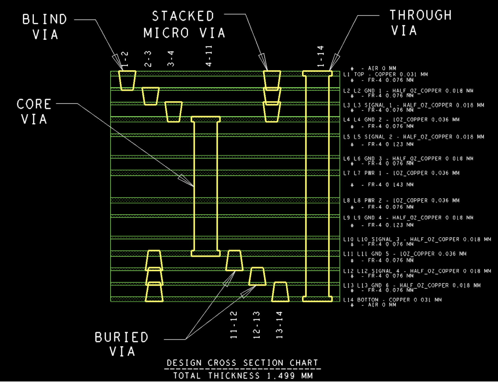
Image Credit: Author - Vias come in many flavors as shown here.
The beauty of a microvia is that it can be used within the SMD pad. Precious space that would be taken by fan-out vias can be used for more components. Via-in-Pad technology is mainstream for RF and digital alike. Shorter inductive loops are possible for the decoupling capacitors using via-in-pad technology. Using a finish of ENIG (Electroless Nickel, Immersion Gold) is common because flatness is improved. A flat pad provides a more consistent solder joint. Power devices or, really, anything with a ground pad benefits from using micro-via-in-pad solutions.
It comes back to the aspect ratio. A via made by a laser has to be wider than it is deep. That means that the dielectric has to be thinner in order to make a useful via size. HDI (High-Density Interconnect) is defined by this process. In today’s world, a PCB Designer will do well to master the intricacies of micro-electronics. There will always be through-hole applications but the balance has shifted towards the shallow end of the pool. Jump in with care.