PCB Design For Laptops and Tablets
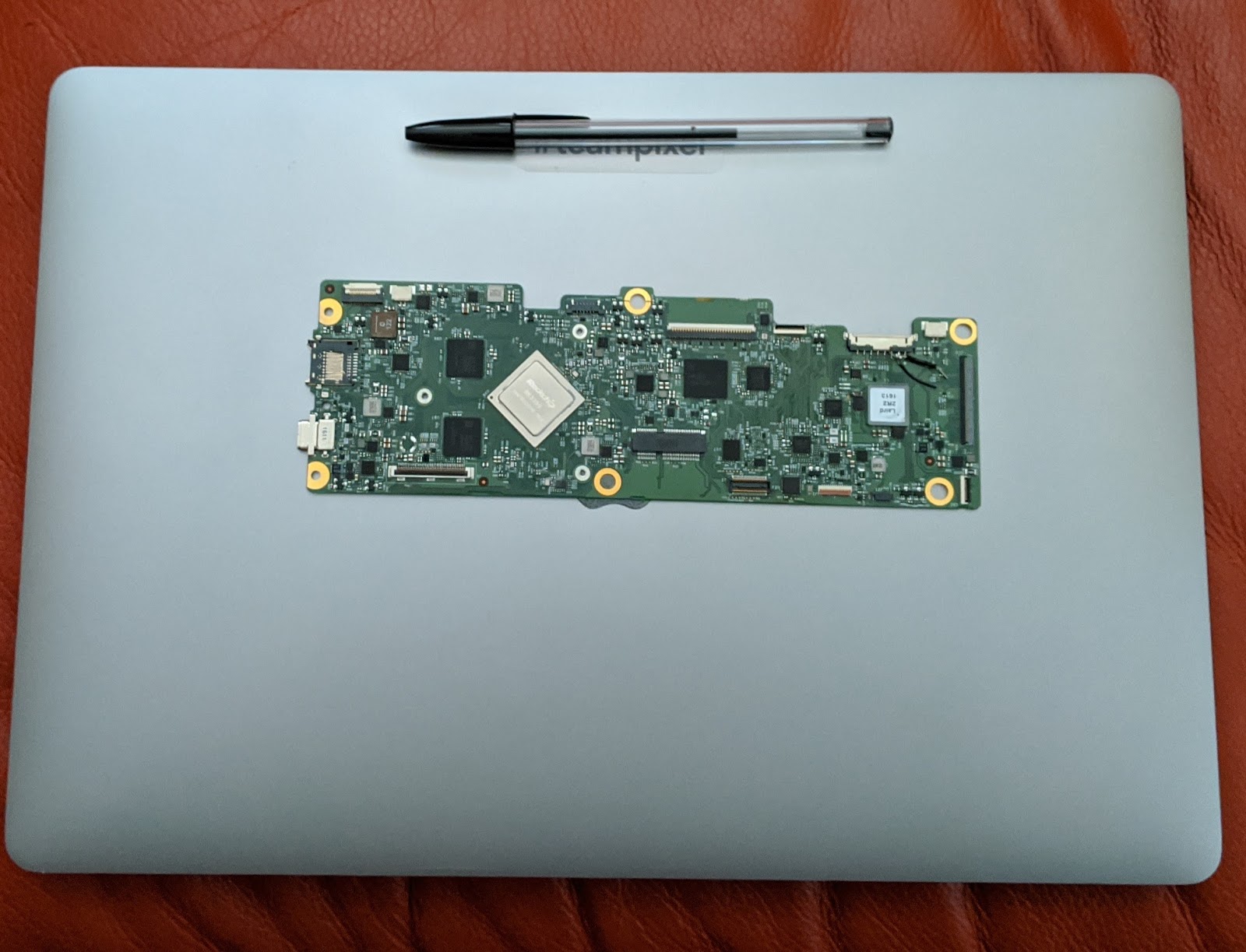
Image Credit: Author - Batteries make up at least half of the volume of a portable computer.
It seems that the consumer electronics industry is trying to get us to use our voices to interact with technology. Screens and keyboards aren’t on that roadmap. Laptops and tablets are not the next big thing. Fine; a declining market is still a market. The standard ATX enclosure for personal computing was downsized to a mini-tower and then went to laptops which became more powerful while also shedding bulk. The product morphed again by losing the hinge and the keyboard. The lines blur as tablets added screen sizes and phones went XL on us.
For all of that, video gamers still clamor for the big old case full of different printed circuit boards. Road warriors in sales need a device that can drive a presentation and fold away until next time. Modern parents still take advantage of the electronic babysitters to occupy their youngsters while they can actually get something done during the day. So, let’s dive right into the Main Logic Board (MLB).

Image Credit: Author - USB type C and SD Card readers are common interfaces.
A System on a Chip (SOC) or a System in a Package (SIP) or a Microcontroller?
The acronyms we throw around help us distinguish the architecture of what we once called the CPU which, if you’ve forgotten, stands for “central processing unit”. Modern chips have a number of CPUs though we refer to them as cores. Multiple cores can be dedicated to general compute tasks while others are geared for image processing or something else entirely. Of course, the trend is towards more of everything; more memory, more bandwidth, more speed, longer battery life, bigger screen, more fun!
The counter-trend is less of everything; lower power and lower temperature rise while taking up less space (except for screen size!) and with a lower weight. We have to deal with this dichotomy while achieving a smaller EMI footprint and avoiding the use of toxic materials or processes. A lot of that work is done for us by the chip makers. The rest is up to us.
In an effort to bring the smallest possible package to the marketplace, the chip team starts believing the world ends at the edge of their silicon. The job of getting all of that power into the chip while getting the data out has landed on the plate of the PCB Designer. Wafer-scale packaging is where the path from the flip-chip or wire-bond cage to the solder pad is a via straight through the substrate.
There is no fan-out going on where a regular through-hole PCB layout will get the job done. The entire industry has had to change in order to get us to where we are now. It will do so again. Mobile processors require high density interconnect PCBs.
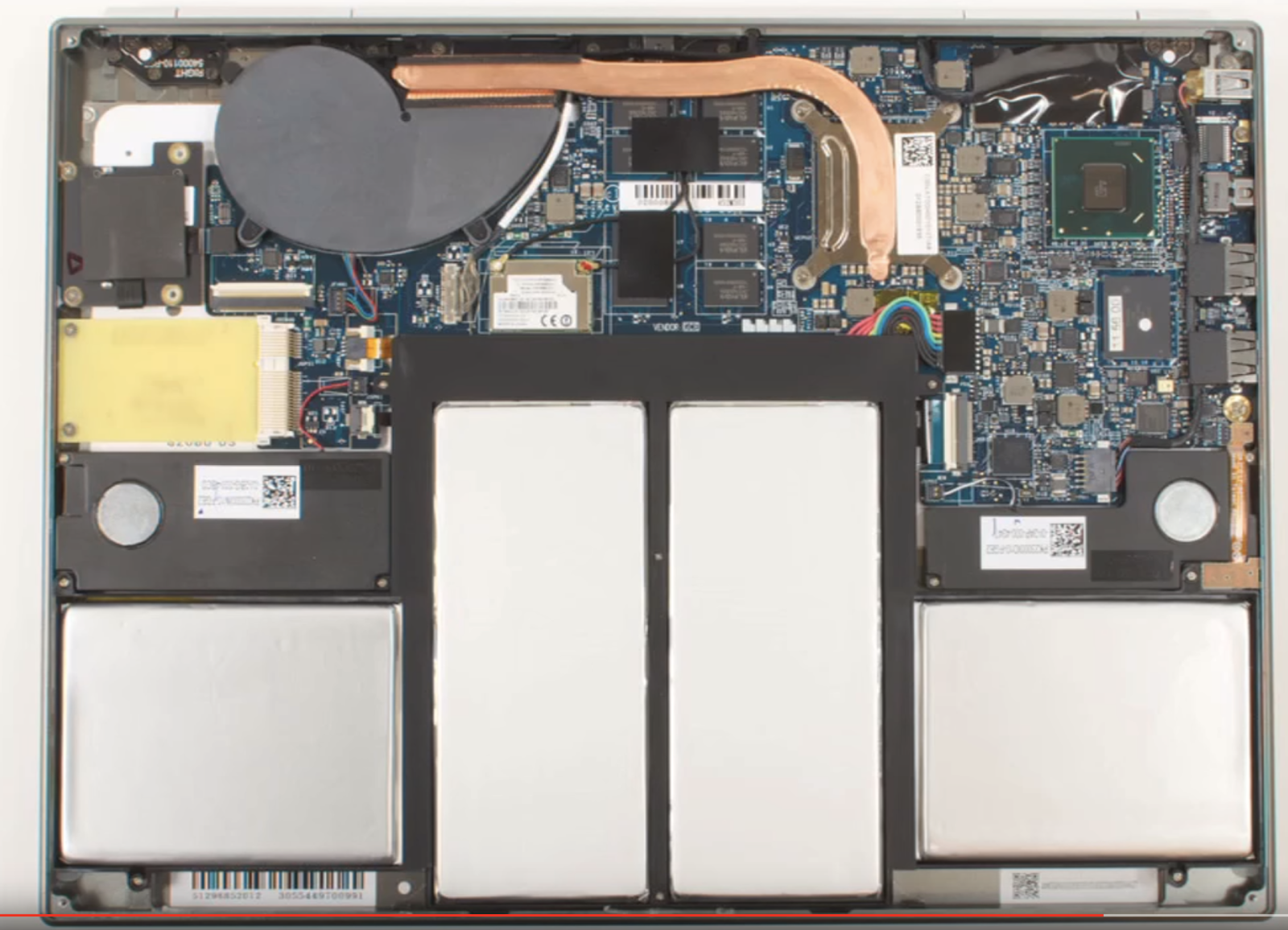
Image credit: Google - The PCB wraps around the batteries and brings everything else to life.
Placement of Components Around the Compute Device
Before you ever see the layout, you have a book to read. One of my favorites was the one about Intel’s Skylake device. The first 200 pages were good but the next 200 were about every conceivable DDR configuration. Now, you’re half-way through the hardware version. Software gets its own 800 pages. It doesn’t matter, Samsung Exynos, Qualcomm Snapdragon, they’re all going to have a data “sheet” that goes on and on.
Some of the instructions can be aspirational. Here’s one from Qualcomm. Keep the area around the device free of other devices and flood ground with via stitching all around the device. Space like that would be space for more batteries. As it works out, nearly every team will insist that their circuitry will need to be close to the main chip. Distance works against signal integrity. The more robust devices will be the ones placed further away from the brain.
Priority Placement and Routing
The top five items on this list all want to be near the processor. Different reasons are in play regarding proximity having mostly to do with aggressors and victims. Use your judgement with regard to your exact requirements.
-
Memory is a given. DRAM and flash have their places determined by the ball-map. There will be power planes that are specific to the memory area and other signals need to stay away. If your system does not have on-die termination, then your termination resistors will demark the boundary of the memory area. I would route and tune the DDR blocks before proceeding with any further placement but that’s just me. EMMC, SPI or other flash memory is notable for large packages relative to pin-count.
-
Bypass caps. Basically, the bottom of the board below the device will be a field of small bypass capacitors. There are caps with three pins with a ground pin between two hot pins. They seem good in theory but can be difficult to implement in large numbers. Just the same, a whole schematic page dedicated to shunt caps is not uncommon.
-
Power Management Integrated Circuit: A fancy name (PMIC) for a bunch of voltage regulators, usually the switch-mode power supplies and their infamous inductors. There are a lot of different functions taking place in a system. Even if the camera(s) can operate at the same voltage as the WiFi, they would never get their 3.3 Volts from the same source.
-
Crystals: There’s always one external oscillator to go with the device’s internal clock. It may only be a kilohertz signal but the rise time creates some hard edges. The crystal for the PMIC may take a back seat to the inductors. Form factors may force a location away from the pins. Route the lines to and from the crystal with care.
-
Analog circuits: Short is the watch-word for 50 Ohm traces. Since they prefer top side routing, it’s even more important to keep them short. Some will likely be buried anyway due to pin location on the device or routed internally to get inside a shield where we keep the analog circuits. In all cases, keep the receive chain away from the crystal. That would be your most vulnerable victim meeting the most aggressive perpetrator.
-
Other things: The pecking order is going to shift depending on who is in the room. Some functions actually do not mind being away from the action. A pull-up resistor can generally go wherever it fits. NFC and GPS antennas prefer a pastoral area out in the boonies. The laptop’s keyboard is generally a low-speed interface. The audio codec is using robust, well-known technology. Cameras are usually set into the top of the screen. Various sensors want their own space. Their personal space usually includes all layers in the region. Power to any sensor must be kept as pure as possible.
All of these “other things” are candidates for daughter cards or modules that are connected by flex circuits. One or more sides of the Main Logic Board would be set aside for edge connectors for that purpose. These daughter-cards and flex circuits will have to be created alongside the main logic board.
One way is to do them yourself. A better idea is to get some help. The MLB will keep a designer occupied. Flex circuits seem simple on the surface but they become iterative along with the physical design and have extra details to sort out with the stack-up. The daughter cards are good tasks for someone coming up to speed. At any given time, a designer will wear a hat that fits.