Optimizing DFA PCB Designs With OrCAD X
Key Takeaways
-
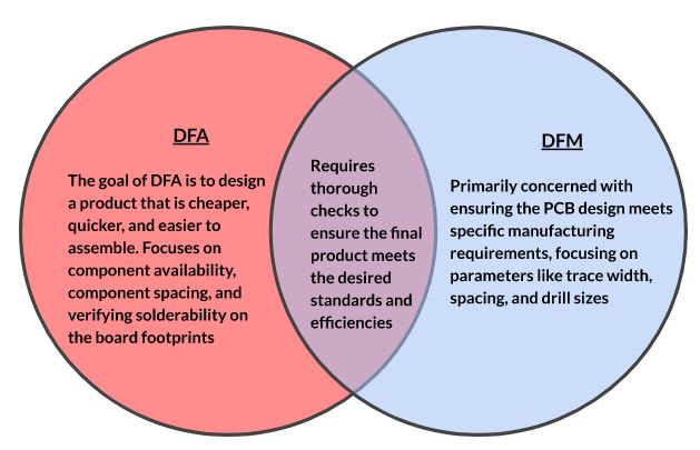
While DFM focuses on meeting manufacturing specifications, DFA emphasizes easing the assembly process to reduce costs and errors.
-
Adhering to detailed DFA guidelines such as pad size, solder mask clearances, and component spacing ensures the PCB design supports efficient assembly.
-
OrCAD X offers specialized tools, such as the Alignment Guide, Basic DRC, and Constraint Manager, which help maintain necessary design constraints.
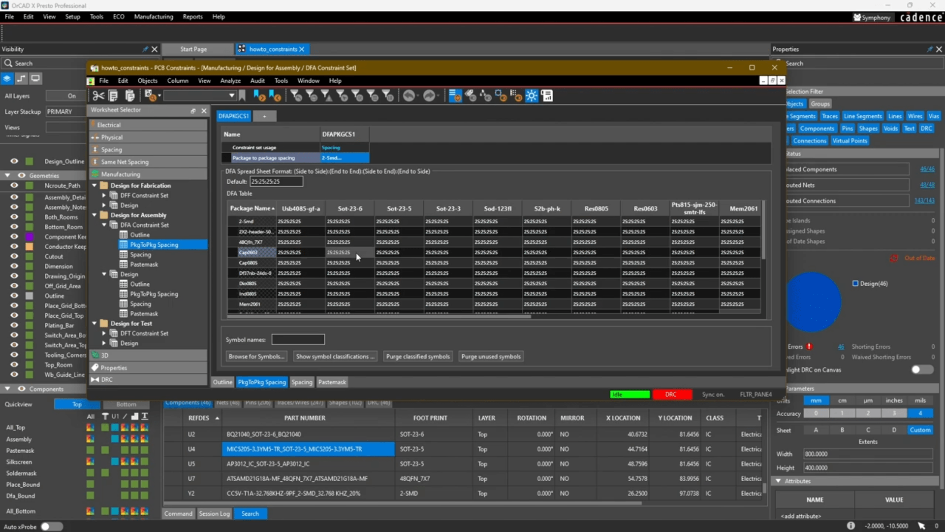
Setting up package-to-package spacing DFA rules
Design for Assembly (DFA) for PCBs is a methodical approach used to guarantee that components on a PCB are assembled accurately and function without errors. Additionally, DFA for PCBs aims to reduce the cost of assembling a board by streamlining its design.
DFA vs. DFM
Design for Assembly (DFA) and Design for Manufacturing (DFM) are complementary approaches in PCB production.
Important PCB DFA Points to Keep in Mind
|
DFA Point |
Description |
|
Component Spacing |
|
|
Solder Mask Clearances |
|
|
Pad Size / Annular Ring |
|
|
Component Orientation |
|
|
Part-to-Edge Spacing |
|
|
Part-to-Hole Spacing |
|
|
Component Clearance |
|
Given the multitude of DFA PCB considerations outlined in the table—from pad sizes and solder mask clearances to component spacing and electromagnetic compatibility—it's evident that manually managing these critical details can be challenging for designers.
This is where the utility of advanced EDA (Electronic Design Automation) software becomes indispensable. Investing in a capable EDA tool that supports comprehensive DFA functionalities can significantly streamline the PCB design process. We’ve compiled an array of OrCAD X tools tailored to enhance DFA PCB creation.
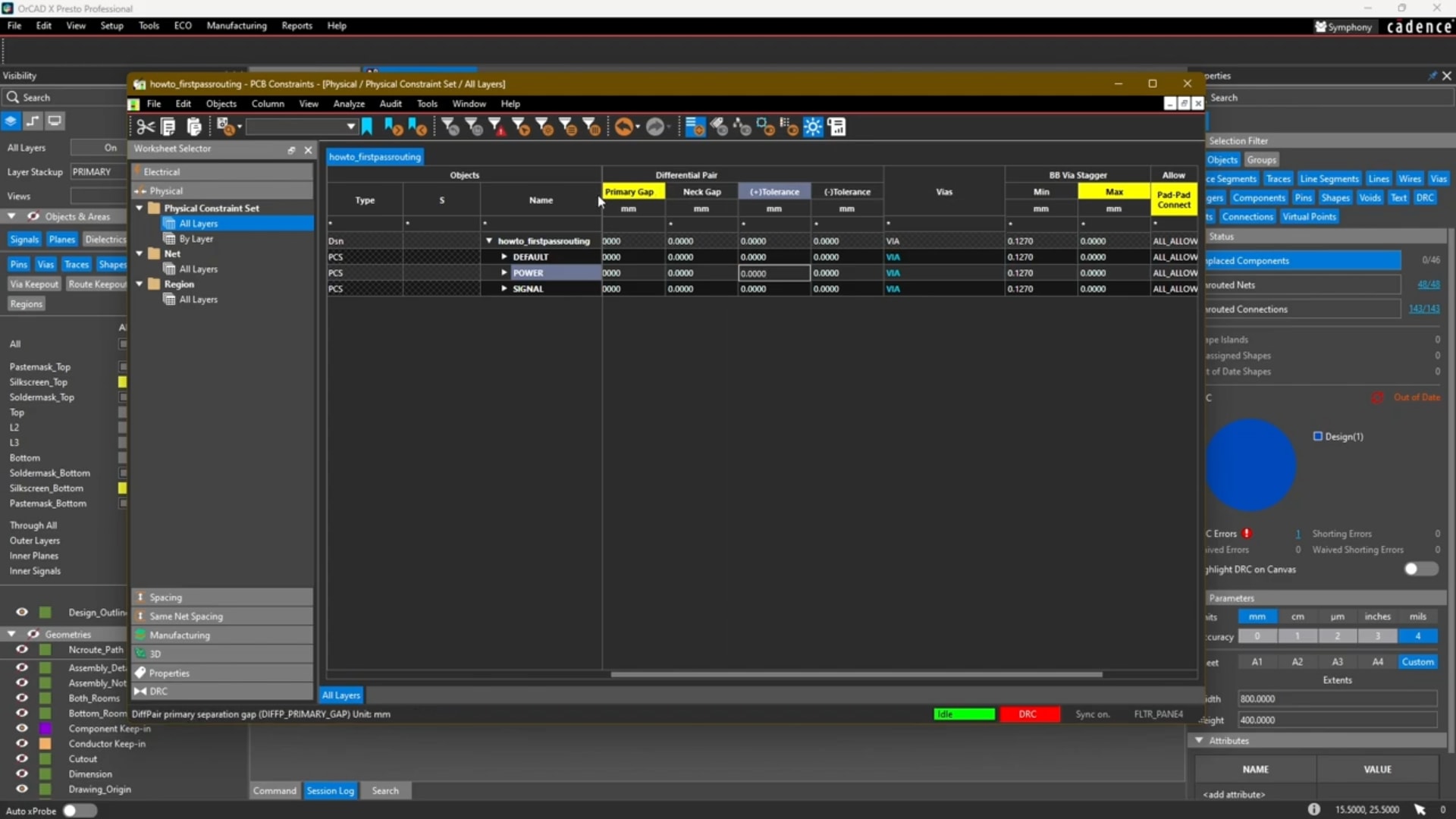
Setting physical constraints in the OrCAD X Constraint Manager
OrCAD X for PCB DFA
|
Tool/Feature |
Description |
How It Assists in DFA |
|
Alignment Guide |
Guides that assist in aligning components on the PCB layout, ensuring that they are positioned correctly relative to one another. |
Helps in maintaining uniform component spacing and orientation, crucial for automated assembly processes like pick-and-place machines. |
|
Basic Design Rule Checks (DRC) |
These checks ensure components do not overlap and meet specified clearance requirements according to PCB design standards. |
Prevents component overlaps and ensures adequate spacing, crucial for avoiding assembly errors like solder bridging or misaligned parts. |
|
Constraint Manager |
A comprehensive tool within OrCAD X that allows designers to set up and manage various design constraints, including those for DFA, to ensure the PCB design adheres to assembly requirements. |
The Constraint Manager is essential for setting and managing DFA constraints such as spacing between components and ensuring components fit properly during the assembly process. |
|
DFA Constraint Set Section |
A specific section within the Constraint Manager dedicated to defining and managing DFA constraints such as spacing between component packages. |
Enables the creation and application of precise spacing rules, ensuring that components have enough space for assembly tools to operate effectively and for manual soldering processes. |
|
Analysis Mode |
A feature within the Constraint Manager that enables or disables the active checking of DFA rules during the design process. |
Facilitates real-time compliance monitoring with DFA rules, identifying and resolving potential spacing issues before the manufacturing stage. |
|
Package to Package Spacing |
A DFA constraint that specifies the minimum distances between different component packages to prevent physical and electrical interference during assembly. |
Essential for maintaining optimal spacing, directly affecting assembly process reliability and the functionality of the assembled PCB. |
|
DFA Package Classification |
A system for categorizing similar components into classes to which specific DFA rules can be uniformly applied, simplifying the management of these rules across the PCB design. |
Grouping similar components, such as all chips or connectors, streamlines the application of DFA rules. This reduces complexity in setting individual spacing rules and enhances overall design efficiency. |
|
Bumpers and DRC Markers |
Visual indicators in the PCB layout that appear when components are placed too close together and potentially violate established DFA rules. |
Provide immediate visual feedback during component placement, helping designers maintain necessary clearances and avoid DFA violations, which is crucial for effective assembly. |
|
Design Rule Checking (DRC) Window |
An interface that updates in real-time to show potential design violations, allowing designers to inspect and correct issues as they design. |
This window aids in identifying and rectifying spacing or layout errors promptly, ensuring the design adheres to all DFA guidelines before proceeding to production. |
|
3D Visualization and Export |
OrCAD X provides capabilities to export and visualize PCB designs in 3D, facilitating the viewing of the board in different orientations, including bending flex regions and isolating specific areas. |
By visualizing the PCB in 3D, designers can assess the physical layout for potential assembly issues, verify component placements, and ensure adequate spacing and clearance. |
|
Collision Detection |
This feature within the 3D visualization tools allows for the detection of physical overlaps or inadequate clearances between components. |
Collision detection is essential for confirming there is no interference between components, which is crucial for automated assembly processes. |
|
Constraint-Driven Routing |
OrCAD X features an advanced routing engine that is powered by real-time, constraint-driven feedback, allowing for the efficient and accurate connection of traces according to predefined constraints. |
Constraint-driven routing assists in maintaining necessary clearances and alignments per DFA guidelines, ensuring that the routing does not lead to manufacturability or assembly issues. |
To experience the multitude of OrCAD X tools available for DFA PCB creation, sign up for a free trial today and take the first step toward enhancing your design process.
Leading electronics providers rely on Cadence products to optimize power, space, and energy needs for a wide variety of market applications. To learn more about our innovative solutions, talk to our team of experts or subscribe to our YouTube channel.