Managing Grids in PCB Design for Maximum Effect
What You Can Capture
-
The origin of using grids in PCB design.
-
Making the design grid work for you in schematic capture and PCB layout.
-
Design tools that give you the best of both worlds.
The grid used in PCB design CAD tools has some similarities to a city grid plan
The practice of building cities on a grid plan has been around for a long time dating back to ancient places such as Babylon in the 17th century BC. The principle of designing cities using blocks or lots separated by straight streets and intersected at right angles is still in use today. Gridded cities are known for being more easily walkable, navigable, and adaptable when new city blocks are added.
Isn’t it interesting that the benefits that a gridded city plan gives its inhabitants are very similar to the benefits of using a grid in your PCB design CAD tools. With a CAD tool design grid you can more easily work with parts and nets, find your way around the design, and add new circuitry as needed. There are of course many other benefits as well, and we’ll take a look at how managing grids in a PCB design can leverage those benefits in order to help you with your design.
Finding the Grid Origin
Finding the origin of a grid is usually a matter of opening up a menu in your PCB design tools, but instead of jumping into the tools right away, let’s first look at grids historically. Using gridded paper is nothing new. I remember as a child watching my dad sketch out electronic symbols, diagrams of the backyard shed, or even the layout of a model train set on that wonderful paper with the lines on it. Using gridded paper for sketching out schematics is only natural in order to keep your symbols roughly the same size as well as aligned. The wavy appearance of a circuit drawn on a napkin may have a certain organic charm to it, but it can be very difficult to read at times.
Due to creating the first PCB designs by hand, the use of a grid for the layout was very critical. The first thing a designer would do would be to place a sheet of transparent grid material onto the light table followed by multiple layers of mylar to create the design on. With the grid as the base, the designer would then tape down shapes called dollies to represent components on the first layer of mylar. Next, the trace routing was drawn in with colored pencils on the mylar layers above the dollies. Eventually, the pads of the dollies and the colored pencil lines would be covered with custom-sized opaque dots and tape for photoreduction. All of this work was guided by the transparent grid to ensure that the correct size and spacing was maintained.
The early CAD tools were for the most part based on gridded systems, so transitioning hand-taped layouts into PCB design tools was a fairly normal progression for designers. Some of the early systems were limited in their capabilities and power though, and their grid setup and operations were pretty basic. This created a lot of headaches for designers who sometimes simply turned the grids off, which led to even more problems down the line with DRC errors showing up throughout the design. Fortunately the tools in use today, such as the schematic capture and PCB layout system in Cadence Allegro, have plenty of grid options to make the PCB designer’s task much easier. Let’s take a look first at how managing the grid settings can help with schematic capture.
The grid display menu in the Cadence Allegro schematic capture system
How Managing Grids in PCB Design can Help with Your Schematic
There are several ways that proper management of your grids can help while you work within your schematic capture tools starting with your library symbols. The foundation of your schematic will be the symbols that you place on it, and they must be accurate. These symbols must not only be created correctly as far as their appearance and electrical attributes, but they must also be set up to work correctly in the schematic environment. This includes several things such as the size that they are drawn at, their electrical attributes, and of course their grid settings.
The pin grid settings for your symbols must be set so that the symbol pins land correctly on the schematic sheet grid. Altering the pin grid setting may force the part to change its scale on the schematic sheet which could be undesirable. It is important therefore to have a symbol standard to work to so that all of your symbol placement matches each other, and all users can easily pull these symbols from your company library. Most schematic capture systems already have a default setting for their symbol pin grids which works for almost every situation. This default setting also makes it much easier to interface with vendor symbols and third party library services. For more information on setting up schematic libraries, take a look at these rules for schematic symbols.
You also have the ability to set up grids and control how they are displayed while working on schematic sheets. By manipulating these settings you can help yourself as you place symbols and draw nets. Grids can be displayed as dots or lines, and also be set in multiples of the pin grid. You can even disable the display of the grid if you prefer working without seeing it. All of these settings can help you with your schematic creation, and this E-book on understanding schematics can give you more useful information.
Next, we’ll look at PCB layout, where grids can help with your basic manual place and route tasks, as well as lend themselves to more advanced tasks like automatically aligning your components.

PCB Layout and Making the Grids Work for You
As with the schematic, the foundation of the PCB layout is in the component land pattern footprints that you create for it. You can set the units that you are working in to suit your needs, and specify a grid setting that will allow you to easily recreate the footprint from the component datasheet.
By changing your grid as needed while you work, you can easily move pins, text, or other objects to their correct locations. Most tools, like Cadence Allegro, will also give you additional capabilities such as setting grid extents and offsets. These will help you to precisely place objects, which you can also do by manually entering the exact location values of the object while you are editing them.
Once your PCB footprint library is ready you will be ready to place and route your design, and managing your grids can be a real help here as well. PCB layout grids can help your design with the following:
-
Location: Setting up a grid for placement can help you to organize your components in the best possible pattern. Many designers will also alter their grids during placement depending on what group of components that they are working with in order to get the best parts placement for the circuit density. Routing grids are usually separate from placement grids, which gives you the ability to set up for routing channels between parts.
-
Spacing: The design rules of the system will warn you about placing components or traces too close to each other. Using a grid, however, will help you place and route much faster by not having to constantly re-adjust your work when you bump into an off-grid object. Five mil lines and spaces will route very easily using a five mil grid to keep their spacing correct.
-
Alignment: Using a grid can help you to align your component placement which will ultimately give you more space on the board. A long row of termination resistors can throw off other parts placement or routing channels if they aren’t aligned with each other. As you can see in the video above, the advanced placement utilities in Cadence Allegro takes working with a grid to the next level. By giving users the ability to automatically align their component placement, you can get perfectly aligned components as if you placed them all manually on a grid.
Once you get accustomed to managing your grids, you can increase your place and route efficiency to a much higher level. For more information on other ways to increase your efficiency in printed circuit board layout, take a look at the following E-books:
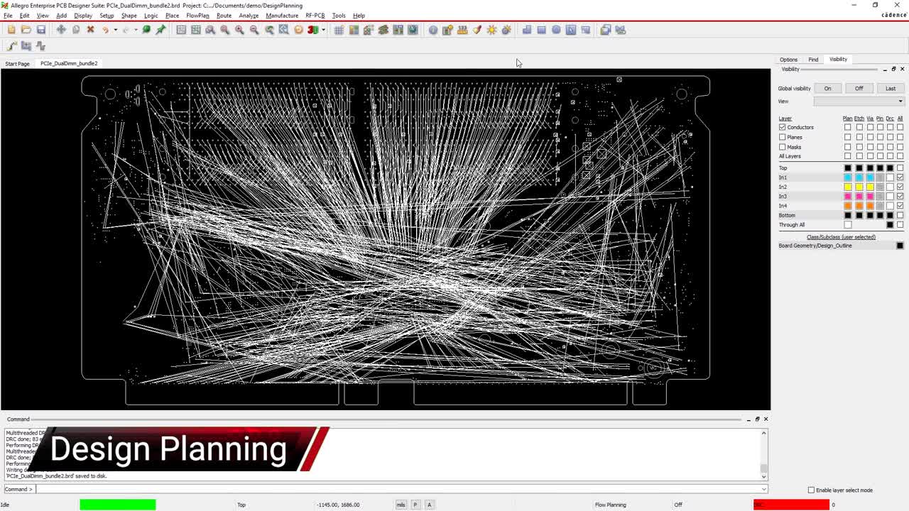
Working with a properly defined grid can help to produce PCB layouts like this
PCB Design Tools that Give You the Best of Both Worlds
As we have seen, learning the best ways to manage your PCB design grids will give you the best results overall. You can keep your designs neat and orderly without the constant need to correct little DRC errors, and you can rest assured that your library symbols and footprints will match your schematics and layouts.
The key is to use the best quality PCB design tools that are designed to give their users the most power and flexibility. Not only will these tools give you the grid options that you need for both schematic capture and PCB layout, but many other features and functions as well.
One of the best PCB design systems available to you today is from the Cadence family of high-performance design and simulation tools. Allegro PCB Designer has all of the different grid capabilities that we have been talking about here. With Allegro you will be able to set up either your schematic or layout with a custom-defined grid that will give you the edge you need in complex PCB design.
If you’re looking to learn more about how Cadence has the solution for you, talk to us and our team of experts.