Free Trials
Free Trials
Read More
10 results found
Featured
Grounding and Return Paths: Advanced Techniques - Part Two
Featured
PCB Design Strategies: Optimizing Mixed Signal Circuit Designs
Featured
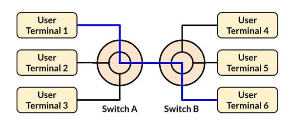
All About Circuit Switching Network Communication
Featured
RF Via Transitions in High-Speed Designs
Featured
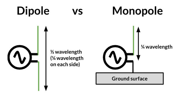
Monopole vs Dipole Antenna
Featured
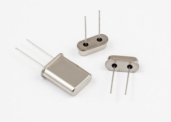
Crystal Oscillator Frequency Ranges and Applications
Featured
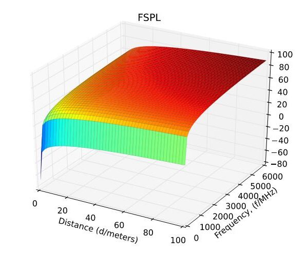
Free-Space Path Loss
Featured
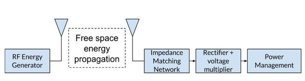
RF Power Harvesting Circuits
Featured
Printed Circuit Board Simulation Technologies
Featured
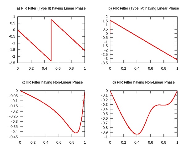
Linear Phase Filters
Featured