Contrary Routing Schemes
It was a warm Saturday morning in late August when we decided to visit my favorite Swedish flatpack furniture store. TM We, of course, means I’m tagging along with my spouse as she chooses some stuff to seal the back-to-school deals. (One more year!) We weren’t the only ones with that plan so it was fortunate that I knew the parking lot well.
The Habitrail Problem
For those of you that don’t know, the store layout -including the garage- is a giant maze of hallways. You’re passing by little rooms of staged furniture on the top floor and then another habitrail running past an assortment of sundry household items on the floor between that one and the parking level. It is supposed to be a treasure hunt with cheap, bland food at either end.
All along these meandering paths, the store has little projectors built into the ceiling that provide arrow shaped beams showing which way to go so you don’t get disoriented. There’s lines of yellow tape for miles. The tour would probably take about 20 minutes if you weren’t shopping. So, walking the crowded habitrail with a shopping cart is easier when everyone is going the same direction. On problem; those renegade shoppers who decide to back-track. That messes up the flow.
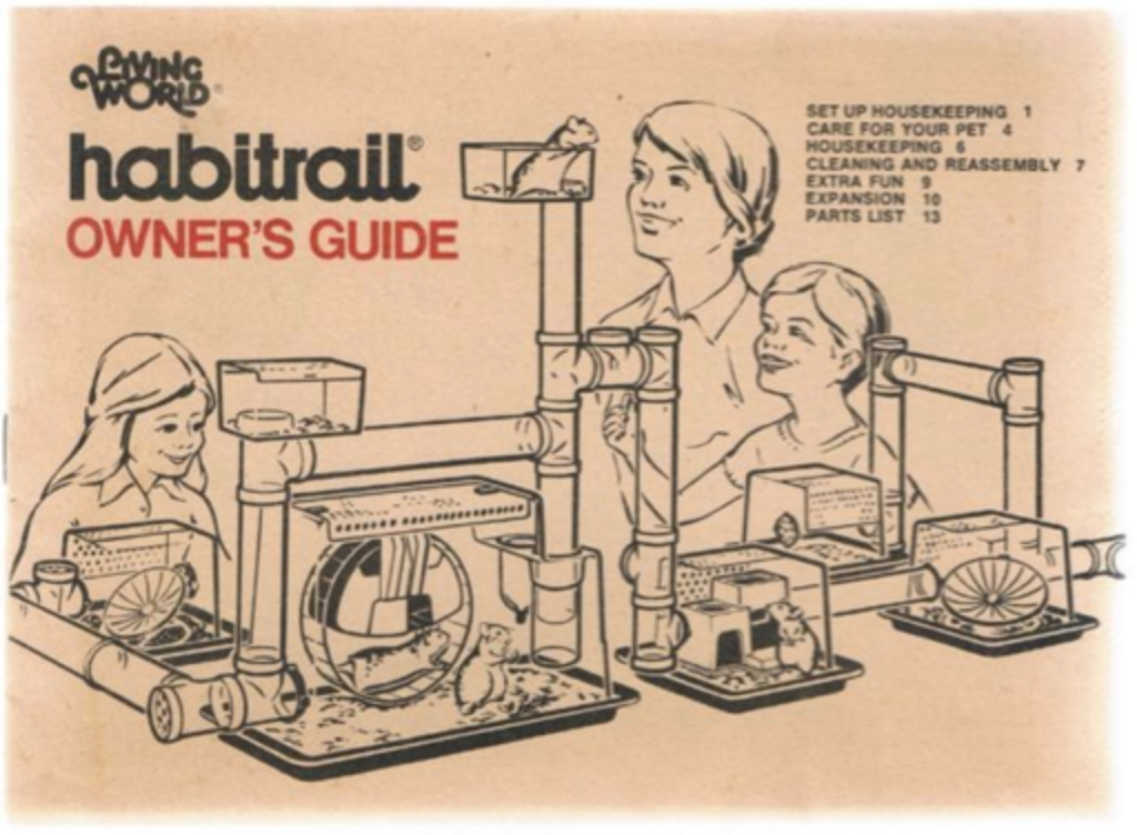
Image Credit: Living World - Hamsters were using vias before vias were cool!
When it comes to printed circuit board design, we are often faced with a few “renegade shoppers”. Once a board has all of the components placed, a tool called rat’s nest shows a line between all of the open connections. From the start, all of them are open and routing is the secret sauce that solves the puzzle. A renegade connection runs counter to the main bias of the design.
Starting at the brains of the operation, it could be a common micro-controller or perhaps a silicon monster with two dozen graphical processor cores. Either way, all of the component locations are chosen based on the best way to communicate with the mother ship. Rivers of connections stand out as dense collections of lines going more or less to the same place. We know what to do with those.
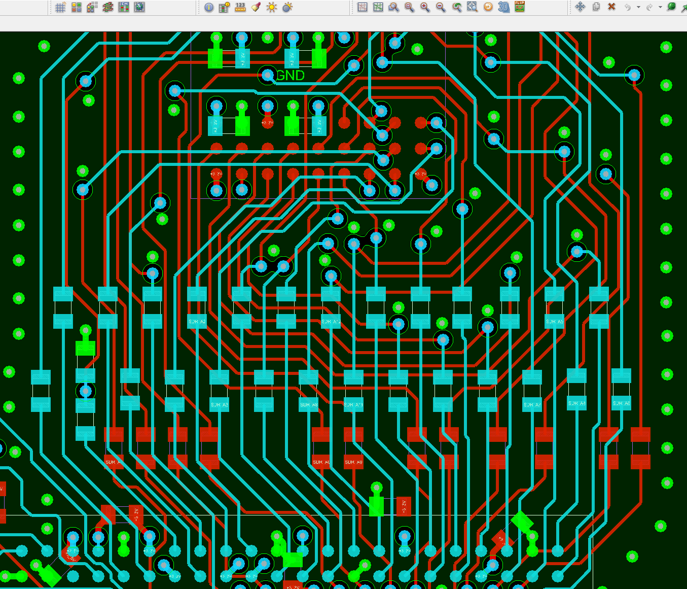
Image Credit: Author - Sorting after the fan-out.
If you’re wondering, route them side by side and clear up the cross-overs by thoughtful fan-out. The idea is to use the layer pair to untangle the data bus. There is usually more latitude to cross over near the secondary device or somewhere in between. There is always a lot of data in the confusion of an un-routed PCB. Routing that SDRAM (above) on two layers including the series resistors looked impossible until a few hours later.
Always present the best I/O by routing away from “the chip”. Let that be the factor that drives component placement. Once all of that is done, it looks like it was a simple and apparent solution. More likely, an elegant board like that took a great deal of effort.
Where to Start?
Circling back to the bare board with rivers of data or smaller collections of traces that seem to go everywhere. Start with the foundational connections that require the most attention. Clocks, differential pairs, any other high bit rate or high frequency routing sets the tone for the general direction of the circuit flow on a by-layer basis. By using the term general direction I hope to steer you towards a conclusion of your own.
You’ve got it, right? A primarily horizontal layer can change its stripes and become a vertical channel out near the perimeter. If your components near the edges tend to use the outer layer to establish a more inboard via location, it becomes possible to skirt past the river of PCIe.
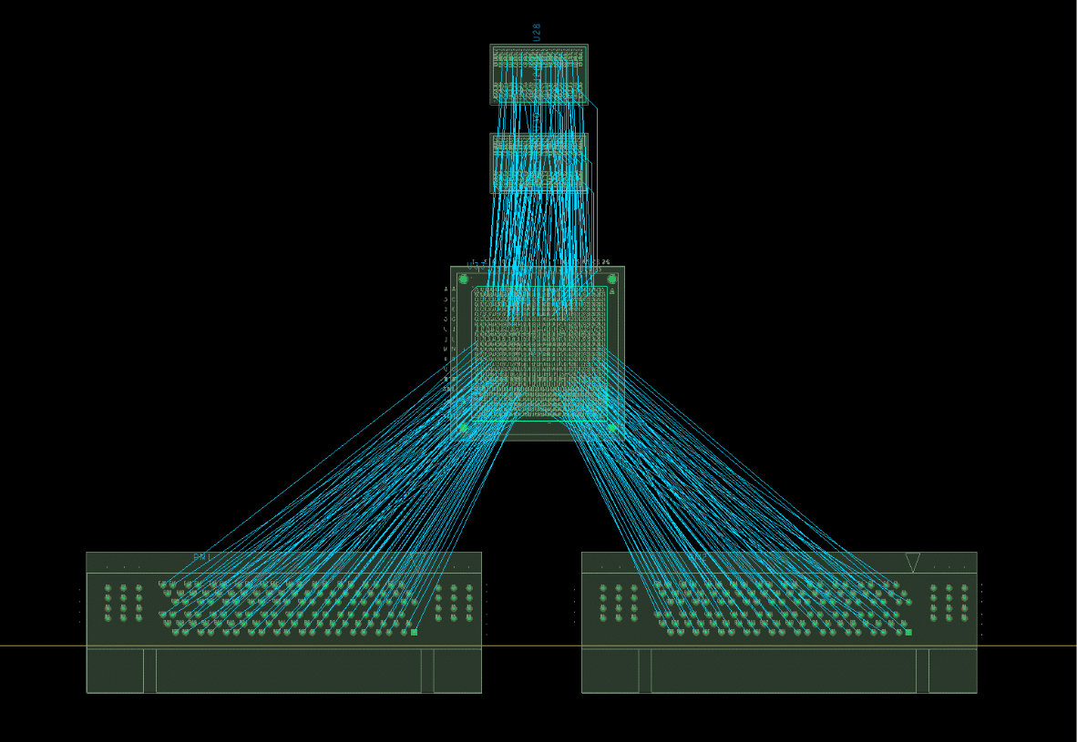
Image Credit: Embedded - We don’t even place the unimportant stuff until this stuff is routed and tuned.
There will typically be some long connections that go from one corner of the board to the other. That diagonal passes right through the chip! Face it. If that connection is important in terms of length, we would have to rethink the placement.
It’s a thing to route, no other rules. From the very start, that trace and its cousins go around the edges. If you were going renegade and routing on a ground plane layer, near the board-edge might be the one safe space place.
One by one, every trace that passes through the gnarly core gets detoured around the hot spot in the rat’s nest. Bit by bit, it starts to become a little more transparent as a web. It becomes manageable and the challenge becomes incorporating improvements as they materialize.
Use Evasive Tactics for the End Game.
Up, down, left, and right; there may only be one direction left for the last GPIO. It is unlikely to be the right direction but we’ll use any port in a storm. A popular plan among our EE patrons is to send an I2C bus around to all of the main chips on the layout. They get to send an all-is-well report back to the brain. “Route this last.”, they say.
Things like your common JTAG bus for functional testing are hard to do wrong in terms of wrecking your test results. The risk is that the routing will cause some effect that wasn’t considered by the SI/PI simulation teams. Clever placement may allow most of those connections to remain on the top or bottom layers from end to end. Components may creep and most likely will have to be moved more than once as the routing demands.
The Final 100 (or 1)
So in conclusion, the edges within the Faraday cage of ground vias present some off-axis opportunities to go around the outside and come back in at the correct routing channel. As PCB aspect ratios favor long skinny boards, we can save precious space in the dense areas by finding an escape route wherever that layer takes you. This can end up saving a layer pair so don’t knock it until you master it. The rouge shoppers are going to make it difficult as they cut across the aisle so a little defensive routing is in order.
The last 100 “unimportant” traces can be disruptive to power and ground planes if the traces hopscotch from layer to layer through vias. Once all of the previously routed critical nets are being digested by the team, we must tread lightly - even when “This one doesn’t matter.”
Components that are placed at a long distance from the center have a chance of being related to a connector or antenna where important things are happening. We have to be mindful of long parallel routing situations. Like when you get to the check-out and there are 26 very long lines to choose from. You’ll get to know your neighbors as you shuffle along. We don’t want our traces getting too friendly. Open another lane.
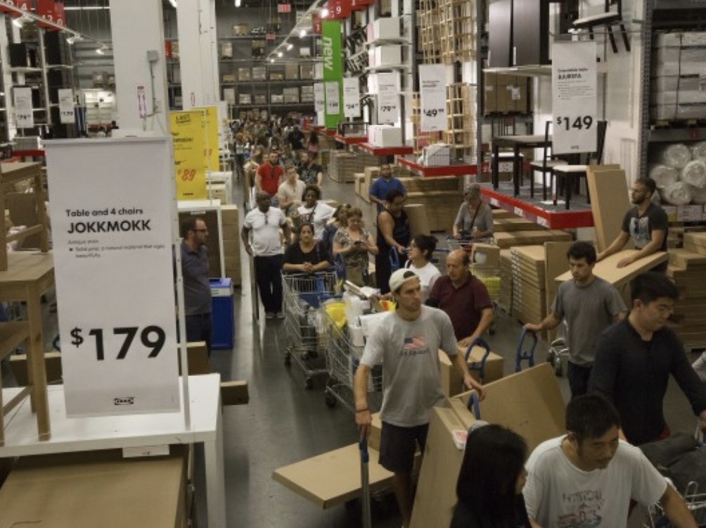
Image Credit: Bloomberg