Considering PCB Assembly Cost And Design Constraints
Key Takeaways
-
Different design constraints affect the cost of PCB assembly
-
How do DfX processes affect PCB Assembly
-
Recommendations for keeping assembly costs down
Imagination and circumstances spur innovation and invention. While this simple statement is true, innovation and invention may not always have a realistic outcome.
Howard Hughes’ invention of the giant H-4 Hercules aircraft serves as an example of imagination and circumstance. A gifted engineer, Hughes responded to the need for quickly moving tanks and troops to the battlefield with imagination. No one had considered building a wooden 400,000 pound flying boat or using eight powerful, 28-cylinder 3,000 horsepower engines to lift the aircraft into the air.
As with PCBs, the design of the H-4 involved moving a concept through the manufacturing process. The story of the H-4 Hercules offers lessons about mechanical size versus cost and whether an immediate need overcomes cost issues. Although on a different scale, manufacturing the H-4 included component placement, conductor cable routing, testing, documentation, and considerations for cost. Due to cost considerations, only one prototype of this behemoth ever made it out of production.
Types of Constraints Affecting Assembly Cost
In our work as PCB design teams, though, we also consider board constraints. Mechanical size stands as a major constraint. While we require enough board area for the circuit and for adequate spacing between components, the mechanical size constraint also brings functionality into the constraint equation. Customer preferences--whether at the consumer, industrial, or military level--and the availability of smaller components also push the mechanical size constraint to new limits.
PCB production processes have limitations in terms of mechanical size and component selection. Those limitations also impact fabricators because of the need to determine via size. While fabricators may wish to work with large vias, some components may require small pitch and higher density components require the use of small vias. Fabricators often prefer to vary via sizes to preserve the integrity of the drilling process.
Despite the many constraints to keep in mind for production timelines and cost efficiency, designers can still be involved and considerate to optimize that process. Guidelines like design for manufacturing, design for assembly, design for fabrication, or overall, design for excellence, all contribute beneficially to the health of your engineering teams’ workflow.
Design for Productivity: DFM, DFF, DFA, and DFX Processes
As you continue to plan your board, additional constraints become apparent. Even if we could convince the general public that a wearable device the size of a large pan-crust pizza is okay, constraints such as size, mounting methods, and clearance impact decisions about layout, component placement, and orientation take us back to mechanical size constraints. Any problems with those decisions often surface during Design for Excellence (DFx) processes.
Fabricators work with design teams towards DFx processes that include methods, guidelines, and standards for producing higher quality products at the concept phase of design. Along with improving quality and productivity, DFx processes also have the purpose of reducing the number of engineering change orders and establishing earlier engagement with component suppliers.
Within the DFx processes, other processes associated with Design for Fabrication (DFF) and Design for Assembly (DFA) standards ensure that the concept for a PCB meets physical layout rules, meet the capability of manufacturers, and ensure that the design meets cost requirements. DFA, for example, examines how stackups and trace widths match with design rules. Design for Fabrication encourages collaboration between fabricators, manufacturers, and design teams for the design of the board.
All those factors impact the form factor of PCBs and decisions about minimum and maximum dimensions. While high-power designs and control applications may require larger-boards, other applications need the smallest possible form factor. DFF and DFA consider dimensions that give the optimal surface areas for a PCB design. Those design processes also study factors such as the board outline tolerance for small PCBs.
How Can I Keep PCB Assembly Costs Down?
Eliminating risk drives project costs down. The early involvement of collaborative efforts in DFx processes identifies possible risks and helps to develop scenarios that reduce risk. In terms of mechanical size, risk involves several factors that include physical integrity, the number of production steps, and tolerance.
Any number of factors can go array in assembly and fabrication, which is why trusting your partner is paramount.
Fabricators have absolute maximum size requirements for a single PCB when using a single panel. Going past those maximum size requirements increases tooling costs and lead time--and impacts time to market. Enlarging the surface area of a PCB also requires additional supports to ensure physical integrity. For fabricators, the use of a large board also can increase the number of steps needed for a PCB assembly project. As an example, a fabricator may decide that a project requires higher cost wave soldering rather than standard reflow soldering.
The use of extremely small boards can drive costs higher because of tolerance, tooling, and handling issues. As an example, design teams must pay increased attention to keep-out layers and keep-out lines. Ignoring those risks could result in the production of a faulty PCB. The smaller boards require additional care during handling and fabrication to achieve the allowable tolerance. Fabricators may also need to design and build custom jigs that facilitate the fabrication and assembly of the boards. Additional costs can occur through the use of supports that minimize stress on the PCB during fabrication and assembly.
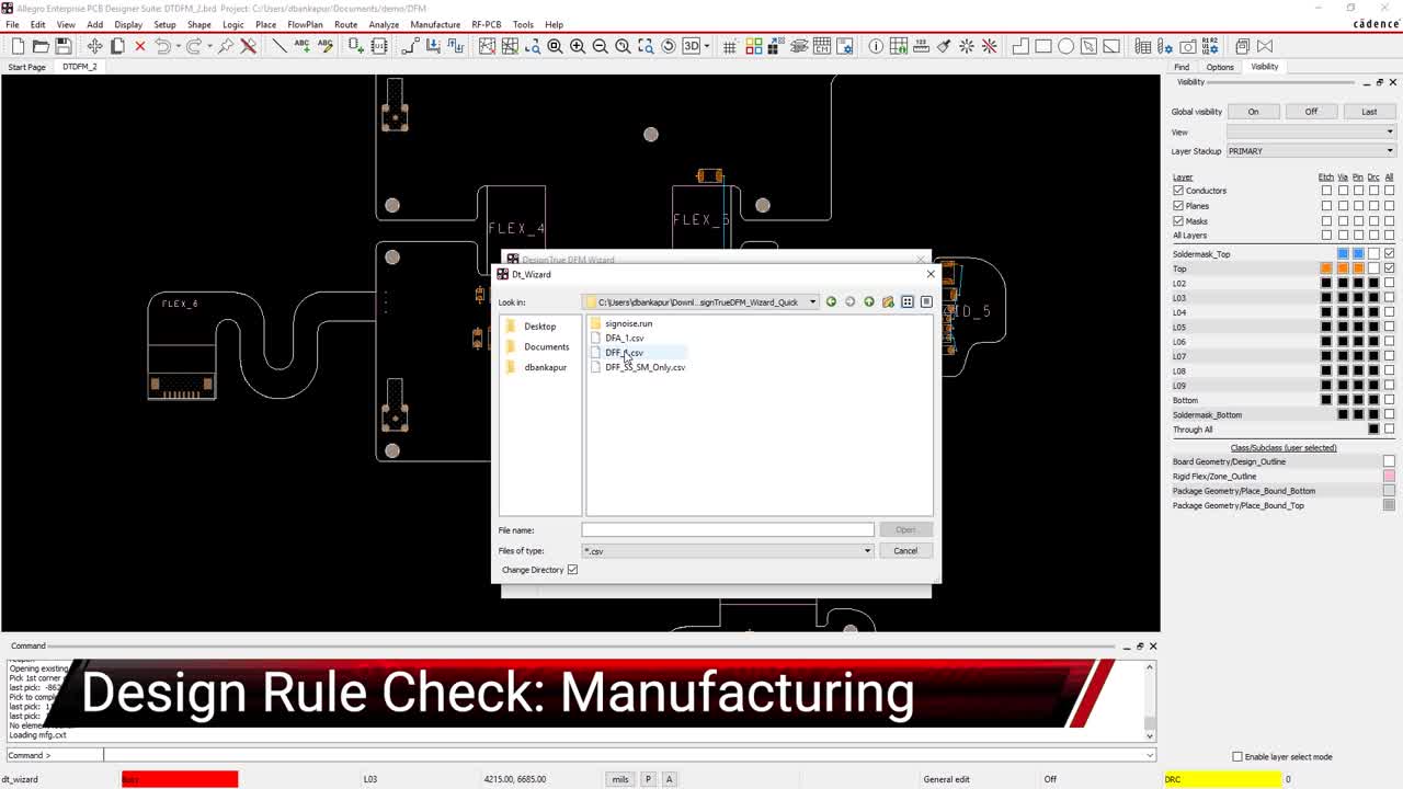
If you’re looking for a PCB design and analysis software that assists your design team in moving an electronic through production, then check out what Cadence offers. What OrCAD PCB Designer can offer any engineering team is seamless team collaboration. Additionally, if you move into Allegro, you gain access to its strong DesignTrue DFM tool to ensure strong adherence to design for manufacturing specifications.
If you’re looking to learn more about how Cadence has the solution for you, talk to us and our team of experts.