CAD Tool Cross-Probing in PCB Design
Cross probing allows you to quickly probe between a schematic and layout (and vice versa).
There’s nothing better than profiting from a “best-kept secret.” For instance, a friend once told me how he learned which day the lake that his family was vacationing at was going to be stocked with trout. He went on to say that no one else was out fishing that day except for his family when the department of fish and wildlife truck pulled up. The driver asked them how the fishing had been as he prepared to release the fish into the lake, and they replied that so far it hadn’t been very good. With a wink, he assured them, “Well, it’s about to get a whole lot better.”
If I had known when reservoirs, lakes, and ponds were stocked like that, I may have had a little more success fishing as well. Another best-kept secret is cross-probing between the schematic and the layout in your PCB design tools. Cross-probing is not a hidden feature, and yet many designers don’t understand or use these capabilities. If CAD tool cross-probing is a secret that you aren’t familiar with, let me explain some of the benefits that it can provide for you.
What Are the Benefits of CAD Tool Cross-Probing in the Schematic?
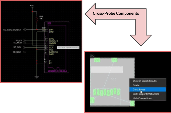
Cross probing is when the schematic and the PCB layout of the same design is set up to work together side by side. A bidirectional connection between the schematic capture and PCB layout tools is opened, which enables design objects selected in one to automatically select their corresponding objects in the other. These design objects can be components, pins, or nets, and when selected in one tool, the other tool will center on the selected object and zoom into it.
For the engineer working in a schematic, this can be a very helpful feature. By selecting circuitry in the layout, the engineer can confirm that the circuitry in the schematic is connected the way that they had intended. Likewise, a component selected in the layout will show up in the schematic as shown in the picture below. Not only does this help with the design of the board, but it is a great advantage during a design review as well.
By selecting U10 in the 3D layout on the right, the corresponding symbol selects on the left
How Cross-Probing Can Help with PCB Layout
While the benefits of cross-probing for design engineers working in the schematic is obvious, the advantages to the PCB layout designer is even greater. Instead of working with long parts lists to find specific components or design notes to specify which nets are sensitive, the layout designer can simply access the schematic for this information. Cross-probing can help the layout designer with many tasks, including the following:
-
Floor planning: Instead of going through a paper copy of the schematic or a printed parts list, cross-probing allows the layout designer to find and select specific groups of parts from the schematic. With these same parts selected over in the layout, it becomes easy to floor plan the design according to different areas of circuitry. For instance, a designer can select all of the components that comprise the power supply of the board in the schematic. On the layout side, the designer can easily group the selected parts in the general area where they are to be placed.
-
Component placement: Sometimes components can get away from a designer in layout during the placement phase. This happens a lot with small parts that are clustered together, and even larger parts can end up on top of each other while being moved around. Instead of searching for the part within the layout, the designer can easily select the part from the schematic that they’ve been using for floor planning, and that part will automatically select in the layout.
-
Routing: When routing traces in layout, it is important to maintain certain clearances and topologies. Even with net name tags and design constraints, it is still helpful for the designer to be able to manually verify which net is which. With the schematic open next to the layout and set up for cross-probing, the layout designer can simply click on any of the different nets in the schematic to do this. Once selected in the schematic, the corresponding net will immediately be highlighted over in the layout.
For those design tools that use a separate utility to manage the design rules and constraints, there is an additional benefit as well. By selecting a net out of the constraint manager, you can see it highlighted in both the schematic and the layout at the same time.
Selecting the group of nets in the schematic, highlights them in the layout and in a 3D view
Put the Power of Advanced PCB Design Tools to Work on Your Next Project
The more advanced the design tools are that you are working with, the more that you can do with cross-probing. We’ve already mentioned how using a constraint manager will give you yet another way to select design objects, and with 3D capabilities in PCB layout, it gets even better.
In the picture above you can see that a group of nets were selected in the schematic, which in turn automatically selected the corresponding net objects in the layout. At that point, we invoked the 3D canvas on the selected objects in layout, and you can see how the routing of these nets is displayed in 3D. This will give you a unique view of how your nets are routed, which can be especially helpful when working with high-speed signal paths.
To leverage the benefits of cross-probing like we’ve shown you though, you need to use a PCB design system that has all of the advanced functions and features that we’ve been describing. An example of a system that has all of these capabilities is OrCAD PCB Designer from Cadence. OrCAD has the schematic capture, PCB layout, constraint manager, and 3D canvas tools all configured to work seamlessly together in order to provide you with a complete set of design tools that will get the job done.
If you’re looking to learn more about how Cadence has the solution for you, talk to us and our team of experts.