Some Key Design Rules for PCB Layout
Key Takeaways
-
Design rules and online checking in PCB design.
-
Setting up the rules and constraints for component placement and trace routing.
-
Using the design rules for 3D checking.
Dense PCB routing like this requires a full set of design rules and constraints to keep it organized
The life lesson that seems to be the most difficult for children to learn is that “rules aren’t there to take away your fun, they’re there to keep you from getting hurt.” And, even if children say they understand this lesson, the next time they roll their eyes because you yelled at them for playing in the street will show that they really didn’t. However, this advice isn’t just for children—it has a very real-world application for circuit board layout designers as well.
PCB design CAD tools have design rules and constraint management systems built into them, and as we tell our kids, the rules are there to keep us from getting hurt. Having a circuit board fail in manufacturing because the components are too close to the edge of the board or because it is too noisy due to the proper trace clearances not being used is extremely frustrating. Design rules are in place to ensure that the circuit boards we lay out will avoid these problems and function as intended. In this article, we are going to look at some of the key design rules for PCB layout that will help you avoid these potential issues.
The Importance of Design Rules and Online Checking in PCB Design
There are many different pieces to the puzzle of designing and building a well-functioning printed circuit board. These include how the parts are placed on the board, how the traces are routed between the parts, and how everything works together electrically to make the board work. The design rules are there to ensure that all of these pieces fit together correctly to complete the puzzle. Design rules can be checked during any portion of the design by running a rules checking command, which will report back to the designer any problems that are found. The rules are also used by the automated online checking system, which will give the designer immediate notice that what they are attempting to move or edit is not allowed by the rules.
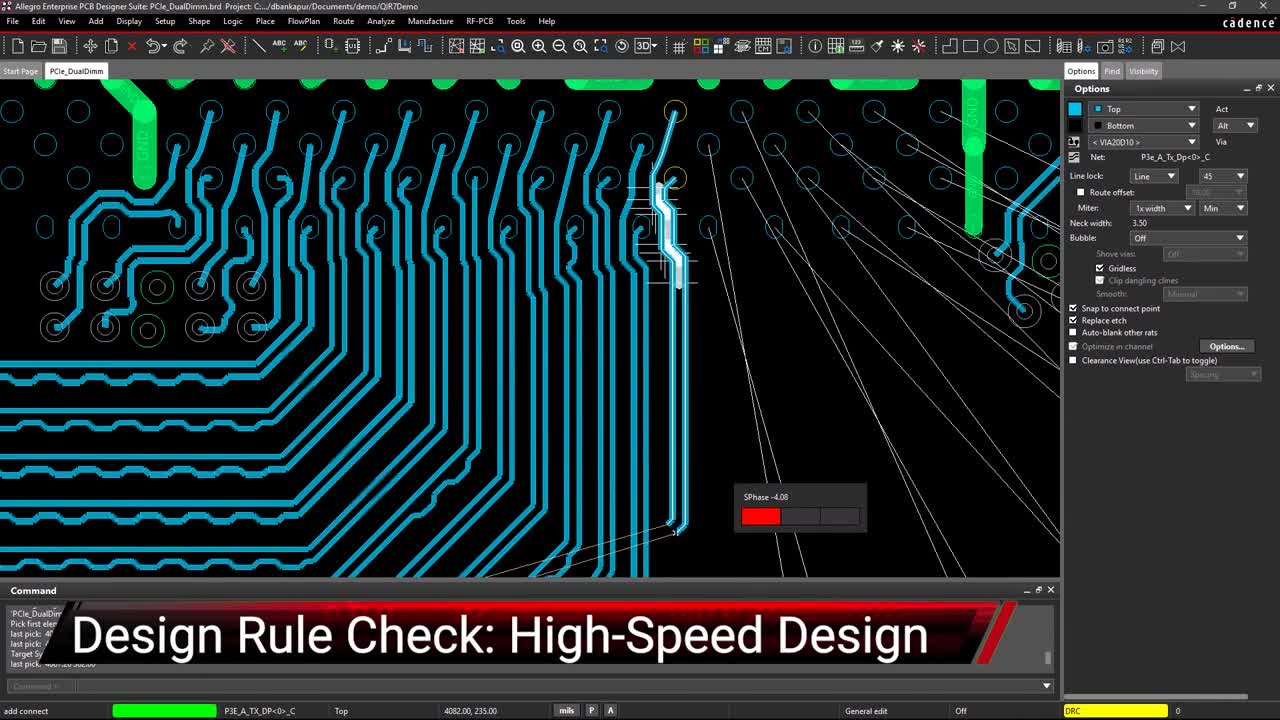
To ensure that the board can be built by PCB fabricators and assemblers, one portion of the rules that can be set up is the design for manufacturability, or DFM, rules. These include unique rules for designing for PCB fabrication, assembly, and test (DFF, DFA, and DFT). They include how close components can get to each other, where testpoints can be placed, and other manufacturing-specific rules. These design rules also allow the layout team to set up the standard, or default, trace routing width, and spacing values. These rules may seem very basic, but they are absolutely essential to successfully laying out the board. The online checking system uses these values while the board is being routed to prevent a designer from accidentally connecting traces that don’t belong together, as you can see in the picture below.
Another part of the design rule system is the electrical constraints that can be added as rules to the design. These control the physical attributes of the trace routing to ensure that the electrical signals arrive at their destination at the correct time, and without being polluted with crosstalk or other signal integrity issues. Here are some of the constraints that can be set up:
-
Measured trace lengths
-
Matching trace lengths
-
Trace routing topologies
-
Differential pair trace routing
-
Layer rules, unique spacing, and specific widths for controlled impedance routing
-
Power net rules for wider widths and clearances
-
High-speed signal paths
-
Trace timing or tuning
Next, let’s look at some of the key design rules for PCB layout, starting with how the rules should begin in the schematic.
Online DRCs keep PCB layout teams from making all kinds of different routing mistakes
An Organized Set of Design Rules and Constraints Starts in the Schematic
The schematic should be captured with a logical design flow of the circuitry on each sheet. Not only is this easier for the PCB layout teams to follow when they lay out the circuitry on the board, but its organization will also help when creating the schematic net classes and design rules. Most design systems give the user a way to create design rules from within the schematic, and you should take full advantage of this if it is available to you. For instance, nets, such as memory buses or impedance controlled lines, can be grouped together in net classes. Although you can apply net rules to a single net, it is a lot easier to apply one set of rules to a whole group. From there you can create specific trace width and spacing rules for layout, or specify certain trace attributes such as topologies or lengths that you want to be followed.
You should also make sure that all of this information is ready to be passed from the schematic to the layout. This means checking to see if all the parts are updated, having the rules in place, and synchronizing the schematic with the PCB layout. This will help the layout team when they use the schematic for cross-probing and the selection of nets and pins. Schematics should also contain notes and information on specific rules and layout requirements. With this data in place, the design is ready for the remainder of its physical rules and constraints to be added by the PCB layout team.
Using design rules and constraints to manage the spacing between component footprints
Getting the Most Out of Your CAD System’s Design Rules for PCB Layout
Each PCB design CAD system will have its own method for setting up design rules and constraints. For our purposes, we are going to use the Constraint Manager in Cadence’s Allegro PCB Editor as our example.
The Constraint Manager is a spreadsheet-style application and is available in both the schematic and PCB editors. In the picture above, the Constraint Manager is being used to set up PCB assembly clearances. These values will dictate how close each component can get to other components or objects on the circuit board. This is critical for component placement to ensure that your final board design is fully manufacturable. In the picture, you can also see the additional assembly constraints that can be set up as well as the menu selections used to set up design rules for PCB fabrication and testing. Here, you will be able to specify rules for solder mask webbing, solder paste coverage, silkscreen coverage, and test point spacing.
In the picture below, you can see the same Constraint Manager being used to set up design rules for trace routing. In this case, vias are being assigned to individual nets, and by expanding the menu, you would be able to see more settings such as trace widths and spacings. These same settings are also available for net classes, layers, or areas. There are also many more constraints that can be added such as trace necking widths, same net spacing, and differential pair spacings. In addition, the Constraint Manager can be used to set up electrical constraints including the following:
-
Signal integrity rules
-
Timing constraints
-
Impedance
-
Propagation delays
-
Return paths
As you can see, there is a lot of data that can be set up in the design rules to help ensure that your circuit board will be designed correctly and can be manufactured without problems. However, in addition to all of that, there are even more key design rules for PCB layout that you can work with, and we will look at those next.
Physical net constraints showing different via assignments in the Allegro Constraint Manager
Taking Design Rules and Constraints to the Next Level
With the use of 3D step models, layout teams now have a perspective of PCB design that used to only be possible with mechanical design systems. With the 3D capabilities of CAD tools, PCB designers have a much fuller and comprehensive view of their work, giving them the unique ability to spot unexpected component conflicts and collisions. These tools also give PCB designers the ability to import mechanical design files to check their board against other elements of the entire system design, including other PCBs, cables, and system enclosures. These systems also have the ability to search for collisions by running design rule checks against the 3D models, as you can see in the picture below.
Object collision reporting in the 3D canvas of Cadence’s Allegro PCB Editor
Design rules for PCB layouts can open up a whole new world by allowing you to push up against the technology envelope, but not go past it. This gives you the freedom to consider all possible scenarios in your design without having to worry whether or not your efforts are in violation of design rules. To find out more about how circuit board design is now converging with mechanical design, check out this E-book from Cadence.
If you’re looking to learn more about how Cadence has the solution for you, talk to us and our team of experts.