Optimizing Your High Frequency PCB Design Layout
Key Takeaways
-
Is there a difference between high frequency PCBs and high speed PCBs?
-
The major challenges for high frequency PCB design.
-
Design guidelines for optimizing your high frequency PCB design layout.
Noise is the bane of high frequency PCB design
While noise is typically associated with the volume of obtrusive sounds, noise can exist at frequencies far outside our range of hearing—which is up to about 20 kHz. In fact, most of what electronics designers and developers would classify as noise can only be seen, on an oscilloscope or similar equipment, and not heard. Whether heard or seen, what we commonly refer to as noise has the same effect: it is intrusive.
For electronic systems that depend on the fidelity of data and information to function properly, noise or electromagnetic interference (EMI) is the primary source of disruption on and between electronic circuit boards. And, for high speed and high frequency PCB design, many of the guiding principles for optimally laying out your board are included strictly to reduce or eliminate onboard EMI and/or achieve the best electromagnetic compatibility (EMC) within the operating environment.
High Frequency PCBs vs. High Speed PCBs
Frequency and speed are often terms that are used synonymously. Let’s clarify the definition of these two terms:
Digital signals, in contrast to analog signals, are not bound to having a consistently repeating cycle. Nevertheless, both analog signal frequency—in s-1 or Hz—and digital signal speed—in bits/s or bytes/s—are measured with respect to time.
The significance of high frequency or speed for electronic circuit boards is the same. That is, “high” means that signal(s) on the board change at a rate such that signal integrity can be significantly affected by impedance and other board parameters. But, just how high is high? For RF signals, impactful signal integrity effects can be observed at frequencies above approximately 50 MHz and extend all the way into the microwave ranges. For digital signals, the answer is not as straightforward.
PCBAs may be classified according to the speed domain within which the fastest signal(s) fall. There are three such domains, as listed below.
Speed Domains
As shown above, if the signal transitions within ¼ of the time it takes to travel the path length, then the board is classified as slow and frequency or speed does not significantly impact the board’s performance or signal integrity. For fast boards, there may be some effect due to frequency. However, this can be mitigated by shortening path lengths. For high speed and high frequency PCB design, there are challenges that must be addressed.
Challenges of High Frequency PCB Design
Designing high frequency PCBAs is similar to designing most other boards in that IPC standards meant to ensure reliability and manufacturability should be followed. However, to ensure that board performance criteria are met, there are a number of additional concerns that arise for high frequency boards, some of which are listed below.
-
Radiation
High frequency and high speed boards often include components that radiate EMI emissions. These devices, such as wireless transmitters, converters, and power supplies, can generate onboard EMI and distort the EMC of the environment where the board is mounted. -
Absorption
Opposite to emitting EMI, your board may be susceptible to absorbing radiation from nearby boards or devices that can affect the performance of your board. -
Signal degradation
A major consideration is limiting signal degradation, which can occur when differential pairs are mismatched, transmission lines are too long, needed shielding is absent, or for other reasons. -
Reflections
Another reason for poor signal integrity is a lack of impedance matching, which can lead to excessive reflections of signals back toward the source instead of being transmitted. -
Coupling
Coupling occurs when two conductors are close together. Obviously, this can have negative effects on signal propagation; therefore, spacing is a very important parameter for your PCB layout design. -
Parasitic capacitance
One of the primary sources of unwanted coupling on your board is due to parasitic capacitance. Although this virtual reactive component cannot be completely eliminated, its effects can be minimized. -
Harmonic distortion
A common source of signal integrity issues is harmonic distortion. Frequency shifts are one of the manifestations that can hamper TX/RX systems. -
Common mode noise
For boards with power supplies and/or conversion circuitry, common mode noise can be a concern. Typically, this is due to the presence of stray capacitance between terminals. -
Surface tracking|
For high voltage and/or current PCBAs, surface tracking—the creation of a current path through degraded insulation—may become a problem. Tracking can be dangerous and lead to burned components or even fires.
The list above is not exhaustive; however, it does clearly show that care must be exercised for high frequency PCB designs.
Creating the Best Layout for Your High Frequency Board
Reviewing the list of considerations in the previous section, it should be clear that creating the best high frequency PCB design layout requires making good decisions in virtually all aspects of your design process. This includes component placement, spacing and clearances, routing, stackup, grounding, and material selection. This can be accomplished by adopting a simple three-step paradigm as described below.
Optimizing High Frequency PCB Design
1. Adopt and Follow Good Guidelines for High Frequency PCB Design
It is important that you adopt a design plan that incorporates proven principles and includes specific actions that address performance, operation, manufacturability, and reliability, as listed below.
- Material selection
- Make sure the dielectric constant is stable for high frequencies
- Use copper with a low profile
- Choose solder masking to minimize the dissipation factor
- Component placement
- Group components according to signal type
- Isolate radiators such as antennas
- Spacing and clearances
- Maintain equal spacing between differential traces
- Follow creepage and clearance standards
- Routing
- Route different signal types on different layers
- Minimize trace lengths
- Maximize spacing between different traces
- Stackup
- Use a symmetric stackup, if possible
- Grounding
- Use separate grounds for different signal types
- Avoid splitting ground planes with signals
- Filtering
- For boards with fast switching, good filtering is critical to reducing EMI
- Shielding
- Use shielding for high radiation components
Following the guidelines above—as well as others that become apparent during design—will ensure that your board meets its performance and operational objectives. However, all selections should fall within the equipment capabilities of your CM’s DFM to ensure manufacturability.
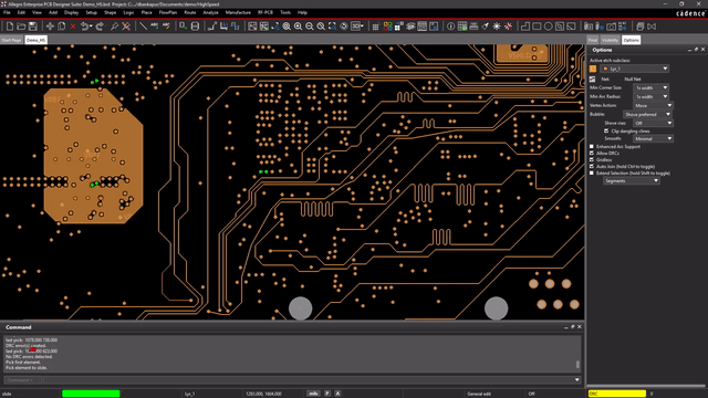
2. Setup and Manage Constraints
Instituting the design rules and guidelines necessary will require setting up a constraint manager, as shown below.
Allegro X PCB design constraint manager
Most of the better PCB design software tools will provide options similar to the ones above for electrical, physical, and manufacturing considerations. The challenge is organizing these such that the most critical have the highest priority. With an advanced design platform such as Cadence’s Allegro X, this is simplified by choosing the high speed option.
Allegro X PCB design focus options
3. Verify Design
The last high frequency PCB design step is to verify your design to make sure that all rule violations have been cleared and selections fall within your CM’s DFM capabilities. It is also recommended that you utilize simulations to test your board’s PDN, thermal profile, and signal flows if this capability is available, as it is with Allegro.
For more information on high speed and/or high frequency PCB design, check out this E-book on common issues that can affect your board’s performance and how to mitigate them.
If you’re looking to learn more about how the Allegro X Design Platform has the solution for you, talk to our team of experts.