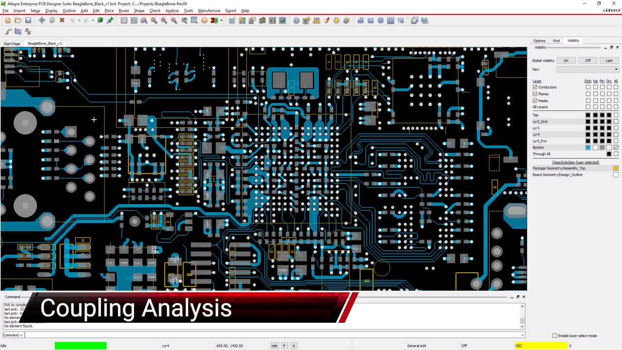
Learn how to quickly identify coupling issues without the need for simulation models or extensive SI expertise.
Other content in this Stream

Here are the problems that can happen to a PCB that isn’t designed for manufacturability, and how an engineer can incorporate good DFM into their design.

This article will give new users a basic understanding of how to set up and use the tools for trace routing with Allegro PCB Editor.

Circuit board viewer tools can help your design department by involving everyone virtually and reducing the amount of paperwork.

Creating a layer stackup in PCB design software takes an understanding of the needs of the design and knowing how to best use the tools at your disposal.

A methodology for providing fast answers to the question of the board technology for a new design.

This article looks at what stripline transmission line routing is, and how you can use your design tools to more effectively route these sensitive traces.

Using power flow calculations to optimize your signals during design, as discussed in this blog, can shave time and costs from your board development process.

Before choosing the best PCB prototyping and fabrication process you need to be aware of the options, which we provide in this blog.

The average power output within a circuit is something that should be adhered to in most cases, and can be designed away from also. Learn more about this process.

Constraint management for impedance control is all about spotting and correcting impedance variations as you route your board.

Communicating with your electronic and mechanical engineers can be challenging and frustrating or it can be easy and a key to the success of your design.

Take a look at the routing for power electronics recommendations we have for you here to get the best performance out of the power supplies on your PCB design.

This article describes how Design for Reliability processes impact component selection and circuit design.

This overview of DDR routing is full of recommendations for your next PCB design involving memory routing.

Here is how you can design PCB layout rules efficiently that will help you to lay out a board design without errors and be ready for manufacturing.

Thermal cycling resistance means you need to prevent conductors from fracturing as a board operates. Here’s how you can ensure reliability.

Signal plane stackups will determine trace impedance, power integrity, and signal integrity. You’ll need to design the right stackup for your digital or analog system.

Not using PCB routing constraints when laying out your printed circuit board can lead to all kinds of different signal integrity and manufacturing problems.

Here are the top five PCB design guidelines for analog circuits that will help you in your mix-circuit PCB designs.

Via-in-pad design is one of the best solutions for routing high-density PCB designs. Here is more information on what VIPs are and how they can be used.