Key Tips for Reliable Rigid-Flex PCB Design
Key Takeaways
-
Learn the specific applications of rigid-flex boards.
-
Where to place vias and route your rigid-flex board for reliable design.
-
Methods to set up an optimized stackup for rigid-flex board design.
Rigid-flex PCB designs require a lot of planning and consideration as to the space and enclosure they will exist in
Rigid-flex PCB design combines the best of both worlds – elements of standard “rigid” (usually FR-4) PCBs with flexible PCBs on a single board. These boards primarily consist of two or more rigid areas connected by flexible polyimide strips with copper cladding substrate. The board fabricator takes the rigid board and then adds through-holes to connect it to the flexible polyimide board.
Due to the complexity of rigid-flex boards, there is a lot that goes into their design. When you apply the design tips and methodologies that we’ll be discussing, you’ll be able to design rigid-flex boards that are reliable and able to withstand hundreds of flex cycles without failure.
Rigid-Flex Boards: Advantages and Applications
Advantages
Rigid-flex boards have become more and more popular due to the demand for compact, shock-resistant, and robust electronics. Rigid-flex boards enable:
- The elimination of connectors
- Increased reliability
- Easier testing
- Saved space
- Better thermal resistance
Connectors
With multiple subcircuits to be connected, connectors are the alternative for transporting power and information through individual subcircuits. These connectors add an additional cost and variable that can cause failure. Connectors are also usually much larger and more involved than the built-in interconnects on rigid-flex boards, which allows for more space to route traces around.
Without interconnects, it becomes significantly easier to probe and automate rigid-flex PCBs, as the subcircuits are already interconnected once the board is manufactured, preventing further waste. If you expect your circuit to be exposed to excessive or repeated shock in high-vibration environments, connectors are more likely to fail. Rigid-flex, on the other hand, is more reliable. With rigid-flex, your board can fold into small profiles, offering significant space-saving opportunities within a small enclosure.
Disadvantages
For rigid-flex PCB design, it’s important to keep in mind some of the disadvantages to truly verify that this design-type is suitable for your application. Specifically, the production process for rigid-flex PCB designs is significantly more complex, which may lead to lower production yields. The manufacturing cycle is also longer, resulting in higher fabrication costs. Rigid-flex boards can also be two or three times the cost of a standard flexible circuit with applied stiffener, although this increased cost can be worth it in particular applications and environments (mentioned below).
Applications
Some key industry applications of rigid-flex designs include:
- Consumer appliances such as ovens and washers
- Telecommunications including routers, servers, and satellites
- Medical equipment: pacemakers, drug delivery, and imaging equipment
- Automotive control systems, air conditioners, and navigation systems
- Industrial test equipment and surveillance systems
- Aerospace sensors and control systems
- Military communications, guidance systems, and tracking systems
Rigid-Flex PCB Design Basics
There is a lot that goes into rigid-flex PCB design. First, consider your application and the advantages and disadvantages previously mentioned. Once you’ve determined that a rigid-flex PCB design is the way to go, consider the board’s intended environment. Is the board meant for a dynamic bend or stable bend, and what is the bending radius?
A dynamic bend rigid-flex PCB is used in an environment where it will be constantly subjected to stresses and bending. In this case, use no more than two layers and ensure that the bending radius is at least 100 times that of the flexible material thickness. Once bent or flexed, a stable bend is meant to remain in that position. In this case, make sure the flexible substrate thickness is about one tenth the bend radius.
Envision your design in the three-dimensional environment it will operate in. A rigid-flex design is usually placed within an enclosure. Consider what mechanical forces and stresses the board may be subject to and ensure that the board within the enclosure is designed to deal with them.
Hole, Routing, and Fill Plane Guidelines for Rigid-Flex PCB Design
Knowing how to route your traces and where to place your vias on a flexible board is crucial for reliable design
When designing rigid-flex boards, the area that is most delicate is the bend. For this reason, avoid placing pads, holes, and vias on these bending areas. Areas near the bending line can apply mechanical stresses that could tear or harm the structure of plated holes close to it. Keep your pads and vias on flexible areas that aren’t subjected to bending, or even better, on the rigid, hard section of the PCB.
If you are placing plated holes or vias on a flexible section, make sure you use anchors to strengthen them as well as a teardrop to connect to any traces. Keep these holes around 10 mils, with at least a 10mil annular ring around them. This larger size allows for easier anchoring and prevents peeling during flexion. In general, avoid placing holes, vias, or pads on flexible areas and place as many as you can on the rigid section. Try to keep them at least 15 mil away from the edge of the stackup, as there can be more instability towards the edge of the board.
Routing for Rigid-Flex Boards
In regard to your traces and routing, keep your traces as straight, perpendicular lines. If your board bends or folds along a horizontal line, then have your traces run vertically. Traces should ideally go in one direction, but in the case where changing directions is a must, curve the traces as opposed to sharp 45 or 90 degree corners. This will eliminate high-stress areas from your board. Use narrower traces that are evenly spread out across a flexible area to decrease areas of high stress. Adding in dummy traces or even redundant traces can help increase the mechanical sturdiness of the flexible areas and protect traces from breaking the signal path completely. In the case of traces on both the top and bottom of a flexible section, alternate them such that a bottom layer trace has no top-layer traces immediately above it, and a top layer trace has no bottom-layer traces immediately below it.
For your power, signal, and ground planes, if you pour a typical plane with a solid area of copper, you’ll end up putting a significantly large amount of stress on your board and reduce its flexibility. Instead, use a hatched-polygon pattern for the plane. Minimize your trace widths on the fill as well, but be aware that a cross-hatch isn’t great for high-speed signal integrity.
Rigid-Flex Board Design Standards
There are numerous standards for rigid-flex boards that are worth consulting. IPC 2223, for example, specifies coverlay construction, adhesive flex cores, air gaps, strain relief filets, and pre-bake requirements for your board. Additionally, it includes tips for the location of plated vias or holes near the transition region from rigid to flex. This area is unique in that the polyimide coverlay which encapsulates the flexible areas must overlap with the rigid areas by a small distance to ensure they are encapsulated by the rigid area of the lamination process. The coverlays are attached to the flex surface with adhesive made out of acrylic or epoxy. If vias are drilled through the adhesive, they can be subject to stresses from the adhesive expanding or contracting due to the high thermal coefficient of expansion, especially during reflow temperatures. IPC 2223 specifies a minimum distance of 0.125”, but many manufacturers can deal with smaller keepout distances.
Stackup and Board Design for Quality Rigid-Flex Boards
When deciding on materials for your rigid-flex board, it’s important to communicate with manufacturers to ensure proper flex behavior. Specifically, pay attention to various mask types, dielectrics, stiffeners, and thickness of copper layers, as these can impact your board’s ability to bend. Make sure to also pay attention to the flammability rating, mechanical considerations, and impedance control for each board.
See the diagram below, which illustrates the stackup of a rigid-flex design structure split into three separate stackups.
-
Primary stackup is the rigid area of the PCB.
-
Stackup zone 2 represents the flexible zone.
-
Stackup zone 3 is also part of the flexible region, but with applied stiffener limiting its ability to bend.
Stackup illustration for rigid-flex PCB with 3 zones: rigid zone (primary), flexible zone (stackup 2), and flex with stiffener zone (stackup 3)
In general, it’s best to sandwich the flex layer between your rigid board, as shown in the diagram. Having the polyimide board as a top or bottom layer can introduce more stress into the system and the adhesion may come off. When designing the outline of your board, having sharp corners can result in tearing, so use your PCB editor’s filet tool to round off any potentially susceptible corners.
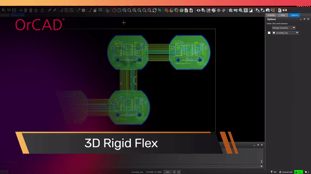
Cadence’s PCB editor includes the ability to create accurate representations of rigid-flex PCB designs. Having multiple stack up zones, bend areas, mask layers, surface finishes, and zone aware placements allows for the creation of high-quality designs. Using stackup zones enables you to automatically have route keepouts to prevent traces from being added into a zone where no conductor layer exists. When placing a component into a zone, the component padstack and geometry can adjust for the zone without necessitating embedded geometries or creating special alternative footprints.