Essential PCB Silkscreen Guidelines for Layout
Key Takeaways
-
The basics of a PCB silkscreen
-
PCB silkscreen guidelines for layout
-
Using the silkscreen features in Cadence’s Allegro PCB Editor
PCB silkscreen reference designators identify the parts on a circuit board
After a collection of our grandmother’s favorite recipes was published in honor of her memory, our family soon discovered that preparing these dishes was a lot harder than expected. The problem was that our grandmother relied on instructions like “use a robin’s egg size amount of butter” or “add molasses until it looks right.” Without clear building instructions, it is next to impossible to cook or manufacture something the way it is intended to be.
In printed circuit board design and manufacturing, we avoid this problem by adding markings on the fabricated board to label the components, specify settings, and even identify the board. These markings are referred to as the silkscreen, thanks to one of the more common methods used to apply the non-conductive epoxy ink to the circuit board. Let’s take a deeper look into what circuit board designers need to know about this labeling process in these PCB silkscreen guidelines.
The Basics of PCB Silkscreen
The silkscreen on a printed circuit board refers to the information and data marked in ink to identify the board and its individual components. Although other applications are used for text markings, and PCB materials such as solder paste may also be screen printed, “silkscreen” has become the industry-accepted term for the PCB information layer. The information conveyed by the silkscreen will vary with each board depending on its needs and application, but, in general, you will find the following categories on most PCBs:
- Component reference designators
- Part outlines or electronic symbols
- Polarity markings
- Probe points
- Pin numbers
- Switch settings
- Board information, including name, part number, and revision
- Manufacturing information
- Legal data, including the company’s name, contact information, and copyright date
Silkscreen information can be applied with different methods, with the following three being the most common:
- Direct printing: Acrylic ink is directly applied to the board from the CAD manufacturing data using an inkjet printer. This method provides the most accurate silkscreen image on the board with the smallest lines and spaces, but it is also the most expensive because each board is processed individually.
- LPI (liquid photo imaging): A photo-imageable liquid epoxy is applied to the entire circuit board using the same process as solder mask application. The silkscreen images are then exposed with a UV light, allowed to cure, and then remain on the board after the unexposed epoxy is washed off. Although not as precise as direct printing, LPI silkscreens are very detailed. Unfortunately, they are also very expensive because of the amount of ink used and setup costs.
- Traditional silkscreening: Using a stencil produced by CAD data as a template, non-conductive ink is pushed through a polyester screen onto the circuit board with a squeegee. This process is very manual, and fabricators must carefully manage the amount of ink, screen mesh, and drying times. Although the most cost-effective application method, this process also produces the least precise images on a circuit board.
Now that we know what goes into manufacturing the silkscreen on a circuit board, the next step is to configure the CAD system for creating the best silkscreen.
Some of the layer and color setups for silkscreens in a PCB CAD system
Configuring the CAD System for Silkscreen Layers
PCB Footprints
The majority of silkscreen information on a circuit board depicts the part outlines of the components on the board and their associated reference designators. Most CAD systems will provide a component editor to add these silkscreen elements to the PCB footprints and patterns. The reference designator in the footprint is usually a generic value that will be replaced by the component's actual designator when used in the PCB layout. Typically, the reference designator is designed to be edited and maneuvered in the layer to place it where it can be seen clearly.
PCB Layout
PCB CAD systems are also set up with different database layers to represent physical layers on the circuit board. You will typically find layers representing the actual layers of the board and layers for solder mask, solder paste, and silkscreens. Usually, there is one layer assigned to the top and bottom silkscreen layers, although some CAD systems will combine multiple layers if necessary for different types of parts. The more advanced CAD systems will also give you separate controls over silkscreen reference designators, component outlines, and other shapes and text. These features allow the operator to turn on and off these different layers and elements as needed for clarity, or assign different colors or fill patterns for added visibility.
In addition to the silkscreen layers, additional CAD layers are usually provided for the following:
- Part outline layers
- Assembly drawing layers
- Test map layers
- Layers with component information other than reference designation
These layers are usually not fabricated into the board but can be used in drawings or simply to aid the designer during PCB layout. It should also be noted that PCB CAD systems usually include full drafting capabilities, allowing designers to add text, lines, shapes, or imported images onto their silkscreen layers. The reference designators and added text and shapes are all part of designers' requirements in standard PCB silkscreen guidelines, which we will look more into next.
This 2D CAD display of etch and silkscreen is the same section of the board as shown above in 3D
PCB Silkscreen Guidelines for Layout
For the best PCB silkscreen results, you should consult your contract manufacturer to find out what they require. However, here are some general guidelines to get you started.
Text Size
The font size and line width of the silkscreen text depend on the type of silkscreen method used for its application. For standard silkscreen printing, you should use as large of font size and line width as possible without going smaller than a 50 mil font size and a 7 mil line. LPI can go down to 4 mil line widths, while direct printing can go down to 3. But remember, just because you can go smaller with your text size doesn’t mean that you should. The smaller the font and line widths, the more difficult they are to print and read.
Location
Reference designators should be as close as possible to the part they are associated with. The more you can keep the reference designators in one rotation, the better, but the designators of smaller discrete parts usually have to be rotated for clarity. However, try to restrict the rotation to 0 and 90 degrees so users won’t have to keep spinning the board round and round to read the next designator. Don’t let reference designators or crucial board information be covered up by components and avoid placing silkscreen over vias and holes. Remember, if you can’t read it on your CAD system, how will the end user read it on the actual circuit board?
Considerations
Many circuit boards have problems because of the following silkscreen errors or omissions, and it pays to look for these conditions and correct them before finalizing the PCB design:
- Mark the polarity of electrolytic capacitors.
- Mark the anodes and cathodes of diodes clearly. In some cases, designers will show the entire diode symbol to omit confusion. Just be sure that the symbol is displayed correctly.
- Be careful about using silkscreen under small discrete parts on the board. It is possible that the bump of the silkscreen ink could affect the soldering of the part.
- Mark the first pin of a connector and note every 10th pin on the connector.
- Label the pin numbers or array of large BGA parts.
- Get your board information correct, including the board name, part number, copyright date, revision, and corporate contact information. Sometimes these values change with board revisions, but the silkscreen isn’t altered to reflect the new values.
Now that we’ve seen some of the important guidelines for PCB silkscreen design, let’s look next at how this work is handled in the Cadence Allegro PCB Editor.
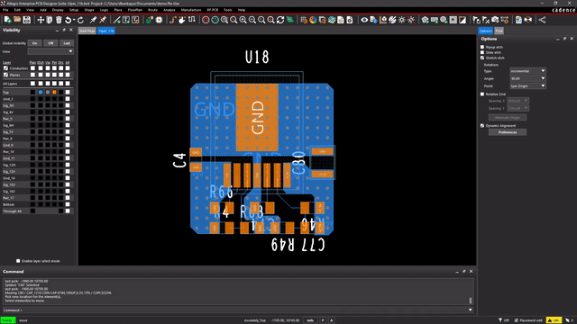
Using the Auto Silkscreen option in Cadence’s Allegro PCB Editor
Silkscreen Tips in Cadence Allegro
Starting with the PCB footprints or land patterns, Allegro gives its users the ability to manually specify the layers and line widths of the silkscreen shape. Allegro’s drafting features will also allow you to maneuver elements, cut and paste, add circles and arcs, and much more while creating the silkscreen. Another option is to use the package symbol wizard in Allegro to automatically create the parts and their associated silkscreen shapes from your specified parameters. Allegro also gives you multiple setups and configuration options for PCB silkscreen layers. You can also change colors, fill patterns, and create additional layers as necessary for your needs.
Once in layout, you can manually edit the silkscreen to maneuver reference designators, text, and added shapes. Another option provided by the Allegro PCB Editor is to use the auto silkscreen mode, as shown in the image above. This function will automatically recreate the silkscreen on a new layer using the existing silkscreen features as a template. It will move reference designators and clear silkscreen from holes and vias, all based on the parameters you set up for it.
For more information on PCB fabrication data and how to successfully get that data to your manufacturer, take a look at this E-book. If you’re looking to learn more about our innovative solutions, talk to our team of experts or subscribe to our YouTube channel.