RF PCB Layout: Transmission Lines, Impedance, and PDN Design
The word “analog” has a special connotation in the PCB design world. One of the things that comes to mind is that we measure performance on a linear scale. We may want to meet a specification calling for 100dB of isolation but we’ll take more if we can get it. The “Internet of Things” (IoT) could also be called the Internet of Analog Things.
This article will discuss the following:
- How the power delivery network affects analog circuits
- Bypass capacitor placement and routing
- Managing Impedance requirements against manufacturability concerns
Sensors come in every flavor under the sun. Measuring heat, light, pressure and anything else in the spectrum falls under the analog umbrella. The smart watch that takes your pulse while sending and receiving radio transmissions from your phone is a good example. The tiny volume of a watch makes it an RF Thunderdome.

Figure 1. Shields within a shield provide for signal integrity for analog blocks. Image Credit: Author
One of the most dramatic agenda items on such a device is supplying power to the chips. It’s an iterative process that whittles the power delivery network down to its bare minimum. Even if there was room to spare, any extra copper for power planes works as an antenna. It’s like taking Occam’s razor to the PDN to reduce the noise floor on the transmission lines. Precise power delivery is a hallmark of compliant analog design.
“Relax, it’s all just a bunch of ones and zeroes.” The preceding words were on a small card on the outside of a cubical of our Test Engineer. The thing is that we were part of an analog chip company that was eventually acquired by Qualcomm. I always found his hands-on work to be interesting, especially when a new board landed in the lab. Going in there was like getting my report card from a class where I struggled for 13 weeks or more.
Star Routing For the Power Delivery Network
I really like a good schematic. It will have copious notes from the electrical engineer. Their goal is (or should be) to hand off the paperwork in a manner that helps the designer through the layout. Notes that provide instructions for which components belong inside which shield will help with placement. Even better is when each bypass cap has a pin assignment rather than just the voltage and ground domains.
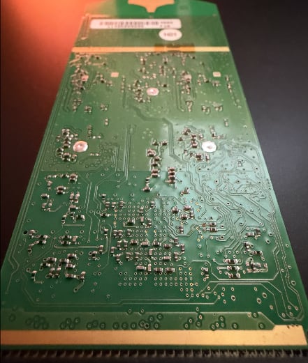
Figure 2. Capacitor placement lends itself to short inductive loops ahead of uniformity of rotation angle. Image Credit: Author
In some cases, it’s more than proximity involved. We’re asked to bring a fat trace to the cap itself and a short, thin line to the assigned pin. Two or more pins could share a cap or multiple caps could be assigned to a single pin. Instead of colorizing the voltage, it helps to highlight individual pins for the capacitors and chips.
It’s not really the intended use case but I would also deploy the “Net Schedule” for tying caps to voltage pins. Its real purpose is for Emitter Coupled Logic (ECL) routing where, for example, you want to ensure that the termination resistors go to the right location. As you move the capacitor around, the rats nest anchors to the desired pin rather than the nearest one.
Impedance Control - The Crux of Analog Design
This is where the fun starts. Our bread and butter is the 50 ohm transmission line. Stripline trace geometry is normally in effect on the outer layers. The key to impedance is line width relative to the distance to the reference plane below and tempered by the dielectric constant (E sub r or D sub k) of the stack-up material. A quick estimate is simply matching the line width to the dielectric thickness. It will be in the ballpark where you can adjust it without breaking things.
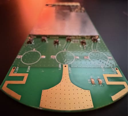
Figure 3. WiFi MIMO printed antennas. The silkscreen circles once had little metal antennas installed. Image Credit: Author
According to IPC-4101/21 the dielectric constant for FR4 is 5.4 but that number can vary by manufacturer; often lower. It also changes over temperature, copper roughness and even the frequency of the signal. I’ve succeeded with this commonly available and cost friendly dielectric material up to 5Ghz. At some point we have to pay up for better material. In addition to the wide tolerances noted above, FR4 becomes lossy at high frequencies.
Impedance Mismatch: The Bane of Signal Integrity
Any “disturbance in the force” is cause for concern. So far, I’ve only discussed outer layer routing. In a perfect world, that’s all that would be used for analog connections. Typically, the placement comes first while the routing follows. In this case, routing beyond what is absolutely necessary is discouraged. Placement and routing go hand in hand.
We want the minimum spacing from the “RF_IN” connector to the blocking cap. Then we want the matching network, usually a pi pad, as close as practical to the DC blocking element. Finally, the amplifier, coupler, or whatever component comes next to be placed so that the trace goes straight, short, and directly to the matching network - all with minimum component spacing.
Sometimes, we need a bit of a transmission line to reach the next item. Anything we can do with the placement to make that line shorter should be done. The components should make up the majority of the path. It bears repeating; we don’t want to see any routing because it’s all radiating on the resonant frequency along with odd multiples thereof.
Considering The Trace vs. Pad Width
We can engineer the stack-up to support a wider line width. The ideal line width would be equal to the width of the pads of the common components. If the pi pad is made out of 0201 resistors, the linewidth should be around 0.35 mm to match the pad. A board using plated through hole (PTH) vias will call for a dielectric thickness in the neighborhood of 0.3 to 0.4 mm for the dielectric material between the outer layer and layer 2.

Figure 4. The RF transmission line from J24 (lower right) flows straight and is only stretched enough to allow for in-circuit test points. Line width matches the component pads. Image Credit: Author
An HDI board creates a complication to this scheme. The size of the microvia determines the dielectric thickness due to the aspect ratio of laser drilled vias. If layer 2 is only 50 micrometers away from layer one, then we would want to clear that layer with a route keep-out and use layer three as the reference plane.
I’ve had to use this routing plan on Chromecast, Hololens and a few other cases. If we were stuck with using layer two as the reference plane, then our outer layer linewidth would shrink below what is manufacturable for typical printed circuit boards. The vendor would have to start with some really thin copper and minimal plating for the via barrels to complete the process. That’s not going to yield a high reliability PCBA.
Where I Use CoPlanar Waveguides
At some point, we have to consider burying the transmission line as a microstrip. Any via creates an onerous impedance mismatch. When I was designing high-power amplifiers for cellular base stations, we managed via transitions with a special geometry that transitioned from stripline to a coplanar waveguide right before the via.
Using a CPWG was said to help through the space between the via and the Layer 2 air gap around the via. The RF signal via could have an enlarged air gap that leaves the top-side trace crossing a measurable distance with no reference plane. The CPWG doesn’t rely on the reference plane below but uses metal along the edge of the trace.
Figure 5. On the right hand side, the stripline narrows while the ground plane closes in to create a CPWG before transitioning to an inner layer so as to cross under the shield The left shows a printed inductor from RF to GND. Image credit: Author
Printing an antenna on the board takes things to another level. All layers under the antenna should be cleared, while copious vias surround the antenna zone. I like to use staggered rows of interstitial vias, three or four rows deep. Analog circuits can be a beast. Thoughtful design practices can tame the beast.