The Art of Stifling Interference on a Printed Circuit Board Assembly
A raging fraternity party with thumping house-music can be really annoying as the morning hours approach. Noise suppression ordinances to the rescue! The partiers have two choices; quiet down or get a citation. The fun-police will also shut down the whole party if it comes to the second choice. Building an electronic circuit has that element in common with the frat-party. If our machines make too much “noise” in any part of the spectrum, it’s game over.
So, while the kids can stop trampling everyone’s lawn and come inside, shut the doors, windows, shutters and even the fireplace flue, we can also contain unwanted spectral emissions. Left unchecked, a printed circuit is an antenna for transmitting and receiving energy from within the board as well as outside.
Figure 1. Image Credit: Author - More participants means more noise.
Even a well designed PCB will have some compromises. Our goal is to be ready to react to any spurious emissions that take us beyond the allowable threshold. We start with a power budget as well as a noise floor and our electronics must comply with those design criteria while meeting regulatory requirements.
As we bring different functions aboard, the problems in the near field multiply. We think of the high speed transmission lines as the focus of our EMI abatement efforts. They are seen as the cause of the problem owing to their signal rise times or a harmonic of that momentary event.
When the root cause is identified, the solution often comes in the form of an additional filter of some kind. Sometimes, that’s not enough and a more extensive respin of the board will have to take place. Just as tall fences make good neighbors, so does putting up some metallic shielding around various circuits on the PCB.
Coupling: That Trace Right There Is Really Noisy. Pass It On!
If nothing else, a frame around a circuit helps define it as a group. Set off by the shield footprint, the part is already on its way to a happy state of affairs. The shield footprint is typically well secured to the inner ground planes by a ring of vias along the perimeter. That’s all part of the 3D faraday cage that suppresses crosstalk within the board itself.
Coupling is a non-linear thing. The amount of coupling that one element will receive from another is a function of the length and width of the gap between the two elements as well as the magnitude and frequency of the signals. With all of that factored in, doubling the gap will square the amount of isolation. That’s a bargain but, of course, it works both ways. Cut the gap in half and the coupling is squared. Yikes!
It would be nice to have an interactive heatmap that showed us the price of rotating an inductor or adding an extra decoupling cap. Right now, that is an outside function known as SI/PI. Signal Integrity/Power Integrity is the branch of engineering that simulates circuits and saves us from making critical mistakes. As the PCB becomes more advanced, making use of SI/PI simulations becomes that much more important.
Coexistence: Making Each Constituent Equally Uncomfortable
The only way to get space for something is to take it from something else. This fact of nature is in play for most power distribution networks. We often have just enough copper to meet the overall power requirements and then only if it is portioned out exactly right.
Figure 2. Image Credit: Author - Generational shrinkage of a WiFi radio over the product life cycle. They are much smaller these days.
Getting the balance right is most important when power is limited. Mobile consumer electronics walk a tightrope of maintaining high performance with low power consumption. Inevitably, the battery grows to crowd the electronics together. When it comes to the final form factor, the shields will cover nearly all of the components as a substitute for the space they had on the breadboard.
After all of the circuits are fully integrated and playing nice together, it’s time to consider the world out there full of other devices. Bottling up the EMI is helped by the metal enclosures with an awareness of the noise sources and the circuit elements that would be most affected by the noise.
Aggressors: The Party Animals of the Electronics World
There are some circuits that we can depend on to be a house-party. One of the characteristics of a noisy circuit element is that they never have a rest state. A crystal will humm along nonstop. A switch mode power supply turns on and off at a certain rate by design. These two players are not usually switching their states all that fast. It’s those harmonics that come into play. Clock traces do the same thing and may not need the help from harmonics - but they get it.
The strategy here is to create a jail that keeps the spurious signals bottled up. For crystals, I like to isolate them with a moat in the copper pour that helps contain their emissions. Not only is the copper pulled well back, there are no nearby ground vias to introduce the crystal to the inner planes.
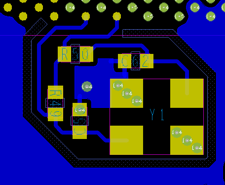
Figure 3. Image Credit: Author - Isolating a crystal’s ground pins from the surrounding copper pour. (I rotated the circuit along with the route-keep-out after this screen grab.)
Layout of a switch mode power supply (SMPS) will feature an inductor on the output pin. The shape that connects the output pin(s) to the inductor is the power supply’s megaphone. That connection has to be short and only wide enough for full power transfer. Aim for a rectangular placement of each power supply sub-section. Voltage conditioning can go near the main supply but individual power supplies should be located nearer their respective loads.
The repeated focus on getting clean power is because a good power distribution network will help cover for some shenanigans on the routing portion of the board. It’s just a fact that some chips will require a few compromises to get through the fan-out.
Victims: Some Circuits Are Designed to Listen and That’s What They Do
If you are already fighting EMI/EMC issues, then it pays to take a good hard look at the power distribution as well as the grounding scheme. Sensors and other similar devices are really good at picking up unwanted interference. In their case, the shield isn’t so much a jail as it is a penthouse where the listening device of whatever type can do its thing in peace.
Receiver circuits are more susceptible than the transmitter side. The higher magnitude of the TX signal raises the noise floor. Most of the traces on a board can be classified as one of the other with I/O lines being a little of both. Locate the sensitive receive circuits as far as practical from the noisy inductors and other culprits. An elegant layout has these attributes as well as provisions to increase isolation should the need arise.
The most common shielding type is the two-piece type that has walls and a lid that presses on over the walls. This allows field service once the shield is installed while the single-piece shield has to be unsoldered from the board for work under the hood. Another way to use a single piece shield is to solder down little clips that hold the shield in place. Is that still a one-piece shield? The companies that make those also make a few standard size covers to plug and play.
Figure 4. Image Credit: Laird - off the shelf shielding solutions with pre-cut “mouse holes”. The crossmembers stiffen the shield walls as well as providing a central pick-up location for automated assembly. The lids can be perforated for airflow.
Of course, a two-piece will cost a little more. You can keep costs down by using a 4-sided shield with 90 degree bends. A six sided L-shape or chamfered edge is not so bad but costs will rise for polygonal shields. It is possible to create multiple pockets within a single shield. These are popular with analog circuits where multiple radios are in use.
Materials are generally stainless steel with aluminum or nickel-silver alloys as the base. The solderable parts will be tinned with other plating possible. Placement considerations are driven by trying to fit into as little space as possible. We have to watch the component headroom under the shield including any webbing and overhang.
On Mouse Holes: To Bury or Not to Bury the Transmission Lines; That is the Question.
Traces can route in or out of the shield on the surface layer through a series of slots located along the base of the wall. Walls with a continuous footprint will require internal routing or cutting out a so-called mouse-hole in the bottom of the wall where a trace can pass under.
Sometimes, the available space demands a special shape for the shield even though we plan ahead for these things. When you are generating a bespoke footprint, it’s a good idea to follow some of the examples by leaving the pattern of mouse-holes so that same shield could potentially be used for other purposes or accommodate future growth.
The height of the mouse hole should be at least as high as the dielectric thickness to the reference plane. The width will consider the trace geometry but also the wavelength if in some circumstances. Guidelines will range from a quarter of a wavelength to a twentieth depending on isolation goals.
The holes in the top of the shield are not just cosmetic or weight savings though they accomplish both of those too. The holes in the top work in concert with the lower slots for convective airflow. Another common feature is a few pegs built into the walls which will require sizable plated through-holes in the board.
Think about clustering aggressors apart from victims during the floor planning and keep the geometry conducive to being corralled by a faraday cage. It is advisable to use the schematic diagram to document the components that will live in which enclosure. The earlier you start thinking about isolating the good citizens from the frat-boys, the better the outcome.