What is Ground Bounce?
Ever wonder why you need a bypass capacitor with a capacitance between 0.01μF and 0.1 μF between the voltage source and ground pins of your transistors and other ICs? The capacitance is so small that some might even be tempted to leave it off. But if you did you might encounter a phenomenon known as ground bounce—a notorious source of noise that can cause problems for your digital circuits. In this post, we’ll introduce ground bounce, what it is, and how to prevent it.
What is ground bounce?
To understand ground bounce, it’s important to understand a bit about how an IC interfaces with your board. In an ideal world, the voltage source and ground of an IC would be identical to the voltage source and ground of the PCB the IC is being installed into. In reality, there exists a small inductance (L) in the leads connecting an IC to your board.
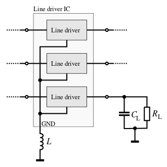
While this inductance is normally negligible, it matters for high speed switching devices such as modern transistors. Recall how in a functioning logic gate, you have a voltage signal that alternates between a high ‘1’ and low ‘0’ state. When the IC is at ‘1’ the output should be at some high value approaching the board voltage. When the IC is at ‘0’ the output should be essentially ground.
There exists the possibility for the local voltage source and ground of an IC to drift from the actual voltage source and ground of your board caused by the inductance of the contacts.This causes the local ground voltage to drift higher than true ground, making your ‘0’ state signal voltage shift upwards. Shift too much, and that ‘0’ could be mistaken for a ‘1’ signal. In other words, that small inductance can have a significant impact on the signal integrity of your board.
How do you prevent ground bounce?
The easiest way to prevent ground bounce is to use a bypass capacitor to provide local charge storage for the transistor. The bypass capacitor prevents voltage from building up between local ground and true ground. It can also be helpful to reduce inductance between ground and true ground by improving the connection with multiple ground pins.
As circuits get faster and smaller, PCB design properties that may have once seemed insignificant can start to become problematic, especially when you introduce high speed signal switching to the mix. Understanding how capacitance, inductance, and other electrical properties are impacted by your layout decisions is the best way to eliminate and prevent noise in your PCB designs. Check out Cadence’s suite of PCB design and analysis tools today.