Sample logo image
Home
Free Trial
Home
Free Trial
    • (2)
    • (1)
    • (1)
    • (1)
    • (1)
    • (1)
    10 results found
    • Sample content thumbnail Featured

    • Sample content thumbnail Featured

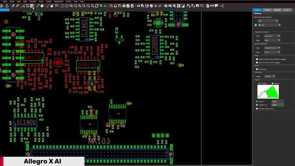
      AI in PCB Design: What Works Today and What Doesn’t

    • Sample content thumbnail Featured

      How to Place Parts from a Component Database in OrCAD X CIP

    • Sample content thumbnail Featured

      Why DDR and PCIe Cause EMI and How to Stop It

    • Sample content thumbnail Featured

      Evaluating EMI Risk in PCB Design Before Hardware Testing

    • Sample content thumbnail Featured

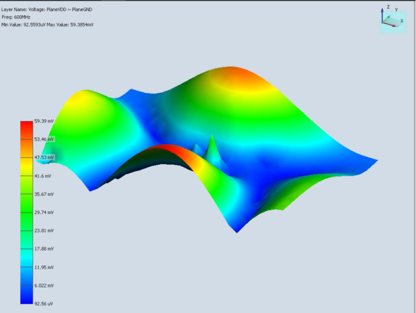
      Power Distribution Noise and Its Impact on EMI in PCB Design

    • Sample content thumbnail Featured

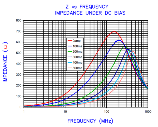
      When Do Ferrite Beads Help or Hurt EMI Performance in PCB Designs?

    • Sample content thumbnail Featured

      Danfoss Uses Cadence Allegro X AI to Amplify PCB Design for Energy Efficiency

    • Sample content thumbnail Featured

      How to Optimize the Electronic New Part Introduction Process for PCB Design

    • Sample content thumbnail Featured

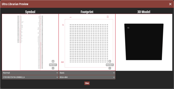
      How to Use Verified Symbols, Footprints, and 3D Models for New Components in OrCAD X CIP

    • Sample content thumbnail Featured

      EMI Reduction Techniques for Switching Power Supply PCB Layouts

    10 results found
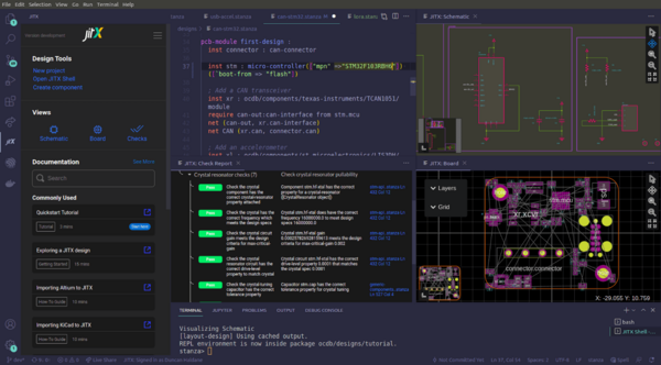
    Sample content thumbnail Featured 
    AI in PCB Design: What Works Today and What Doesn’t
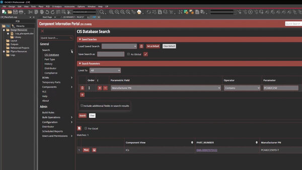
    Sample content thumbnail Featured 
    How to Place Parts from a Component Database in OrCAD X CIP
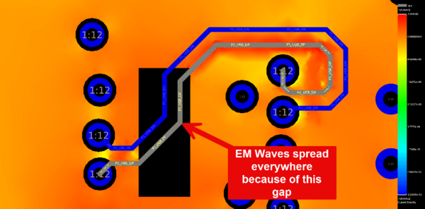
    Sample content thumbnail Featured 
    Why DDR and PCIe Cause EMI and How to Stop It
    Sample content thumbnail Featured 
    Evaluating EMI Risk in PCB Design Before Hardware Testing
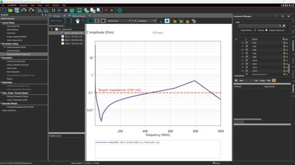
    Sample content thumbnail Featured 
    Power Distribution Noise and Its Impact on EMI in PCB Design
    Sample content thumbnail Featured 
    When Do Ferrite Beads Help or Hurt EMI Performance in PCB Designs?
    Sample content thumbnail Featured 
    Danfoss Uses Cadence Allegro X AI to Amplify PCB Design for Energy Efficiency
    Sample content thumbnail Featured 
    How to Optimize the Electronic New Part Introduction Process for PCB Design
    Sample content thumbnail Featured 
    How to Use Verified Symbols, Footprints, and 3D Models for New Components in OrCAD X CIP
    Sample content thumbnail Featured 
    EMI Reduction Techniques for Switching Power Supply PCB Layouts
    Sample content thumbnail Featured 
    •  (2)
    •  (1)
    •  (1)
    •  (1)
    •  (1)
    •  (1)
    English (US)
    • English
      United States
    • 简体中文
      China
    • 日本語
      Japan
    • 한국어
      Korea
    • 繁體中文
      Taiwan

    © 2026 Cadence Design Systems, Inc.

    • Trademarks
    • Terms of Use
    • Privacy
    • Cookie Policy
    • Accessibility
    • Do Not Sell or Share My Personal Information(opens in a new tab)

    © 2026 Cadence Design Systems, Inc.