How To Maintain Connectivity in a Multiboard PCB System
Bringing a multiboard system together is a chance for the designer to spread their wings. As the circuit spreads, so do the risk of crossed signals. Some of the ways the circuits can get scrambled include:
-
Some connector vendors have clear indications of polarity. Others leave all numbering to the buyer. In the same way, a row of gold fingers will be anything we draw up in terms of pin numbers and signal names.
-
While the physical design typically depicts the orientation of a connector by indicating the location of pin one, rarely is the net that goes on the circuit defined at that level.
-
Each board in the system has a separate schematic, probably drawn up by a subject matter expert that naturally varies from one board to another.
-
A connector can be mirrored to the secondary side, yet we can view it as though we had Superman X-ray vision.
-
A single large connector can have a cable or flexible circuit that mates to it but then splits the larger connector’s signals into several smaller connectors that get distributed all over the system. Each of those branches will have a pin-one of its own but only one of them at the end where everything is collected together.
-
Rogue changes on one card can derail a system.
-
Library inconsistencies and simple mistakes can as well.
Closing all of those potential open loops takes a degree of organization. The system level physical designer is very concerned with everything fitting together. PCB Designers are working within their outline(s) and can also become a bit myopic in that regard. It seems as though we go over these things ad nauseam in the early design reviews when the high-level architecture is being laid out. Then, some bug crops up when we put everything together. What happens? How can we stay on an even keel?
Block it All Out
I don’t mean therapy or hitting your head against the wall. Block Diagrams, Wiring Diagrams, Interconnect Diagrams, Interface Control Diagrams, Outline Drawings, and beautiful 3D renderings all help put the big picture in perspective. They may also be considered too mundane for the critical path and be put off until everything is completely defined. What happens then is that any disconnects get cleaned up in the pre-production run. New boards/cables/flexes are rushed out and all of the expediting and long days go into trying to mitigate the risks before going to mass production. Turning up volume production on something that is mostly tested and verified is one way to live on the edge. So is blindfolded paragliding. Nobody talks about the time their parachute didn’t open. Fewer mistakes in the prototype stage pay the dividend known as peace of mind as we confidently scale up our efforts.
The bigger the job, the more we need to employ risk management in the form of stronger documentation. Nobody does testing and documentation quite like NASA, but the auto industry is really good at supply chain management. When you become part of the supply chain, you quickly become well managed. You get to generate all sorts of documents related to design verification at all levels. Just as you are managed, you become a technical manager to your suppliers as they do for theirs. But I digress.
Creating Order From Chaos, One Step at a Time
The thing is that this level of scrutiny is not as common in the typical consumer hardware setting. Getting your engineering folks to draw up a proper interconnect table may be a stretch. Starting your own “quick and dirty” version is better than nothing and may even prompt the team to fulfill their ideal destiny. We’re after a schematic of schematics. There is a lot of abstraction at this level. A box represents a board, and a list in the box represents the functional connectivity between the various boards.
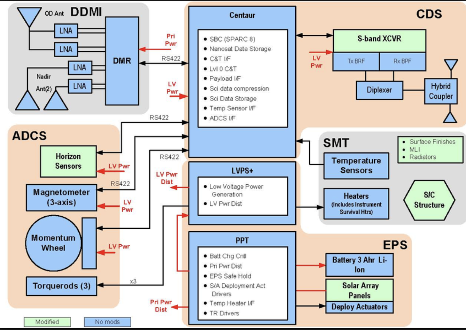
Image credit: Research Gate - Use more or less detail as required
A system power tree is another important reference point. The number of functions a product has will be a close indicator of the different number of power domains required. Let’s say, for instance, that we have a camera and a display to go with a microphone and speakers to make an Arduino conference room package. All five of those items will want their own power supply even when they are designed for the same number of volts. Scale up to the devices with over 1000 pins and each little area of the device wants a particular power source all its own. They give me an 800-page owner’s manual for the Intel Skylake device. You’d shake your head at that ball-map. It does have an excellent power tree along with the reference design material though.
Life on the Analog Frontier
We got the chance to create a reference design for a Samsung Chromebook Plus. We had the main logic board and a handful of outlying boards. GPS, for instance, needed a quiet area so it could receive the small signals from the satellites. I mean quiet in an electromagnetic sense. The speakers still qualify as a problem because of their magnets. The metal enclosure, the WIFI, the Bluetooth and a number of sensors were all problems.
Coexistence is the name of the game when we try to make all of these disparate functions work together. Simulations will take us a long way, but there are blind spots. You don’t know until you have everything packed into the form factor and turn it all on. Who can forget the time that people wrapped their hands around the upper area of the new iPhone and were told that they were “holding it wrong”? The Pixel phone with its band of non-metal color is an indication of where the invisible connections are taking place through various antennas.
The short answer is that wireless connectivity is the risk that is hardest to manage. For the most part, we try to contain electromagnetic waves. In this case, we’re making them on purpose. The more wireless protocols you have, the more corner cases to explore. Life is better if you only have to tame one radio. Your phone is a war zone of conflicting interests. This laptop was no different. The prototypes were not 100% ready for prime time. The project was pulled together with a few schematic revisions including more filters and regulators; small stuff for the P1 stage except for mis-wiring the battery connector! Mass production followed on with minimal drama. I can say that now, but I was 10,000 miles from where most of the action took place. I know they worked hard too.
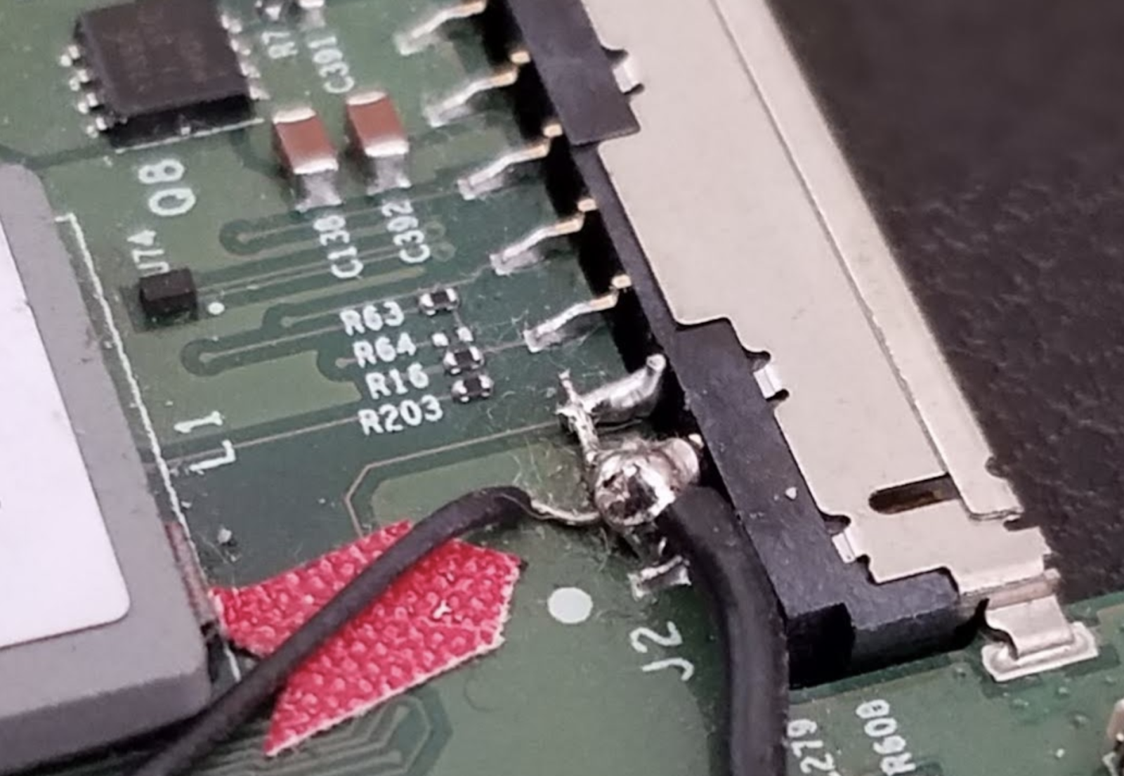
Image credit: Author - You’d think we could do something as simple as a battery connector.
The result was thin, light, fast, robust and flexible enough to wrap itself into a tablet, stylus included. Here is a glowing video review of the hardware. Spoiler: the man spent 12 minutes talking about this one laptop and did not have any negatives. Could it be that good? The awards at CES ‘17 were long and strong. This is the ARM processor version that has a lookalike big brother with the Intel SOC. The reviews tend to reflect that this is the lower tier of the Samsung premium convertibles. Working with the outside vendors on the reference designs was interesting.
They provided very detailed .dxf files so we could import geometry directly to the layout. The inner workings of the laptop were rendered over several layers. In a way, that was even better than drawings. The ODM (original design manufacturer) also had the wherewithal to take on the system interconnect review. Between the software models and mock-up hardware, the away team executed a nice product on a three-spin development cycle. Prototypes are the breadboard version without any physical limitations. Pre-production is the first time all of the components are joined in the form factor, and the third cycle is the one that you can still buy. Or not. I have pride in the work but, Samsung doesn’t share anything with me. They are in-house for their designs anyway. We provided a six-layer option to their eight.
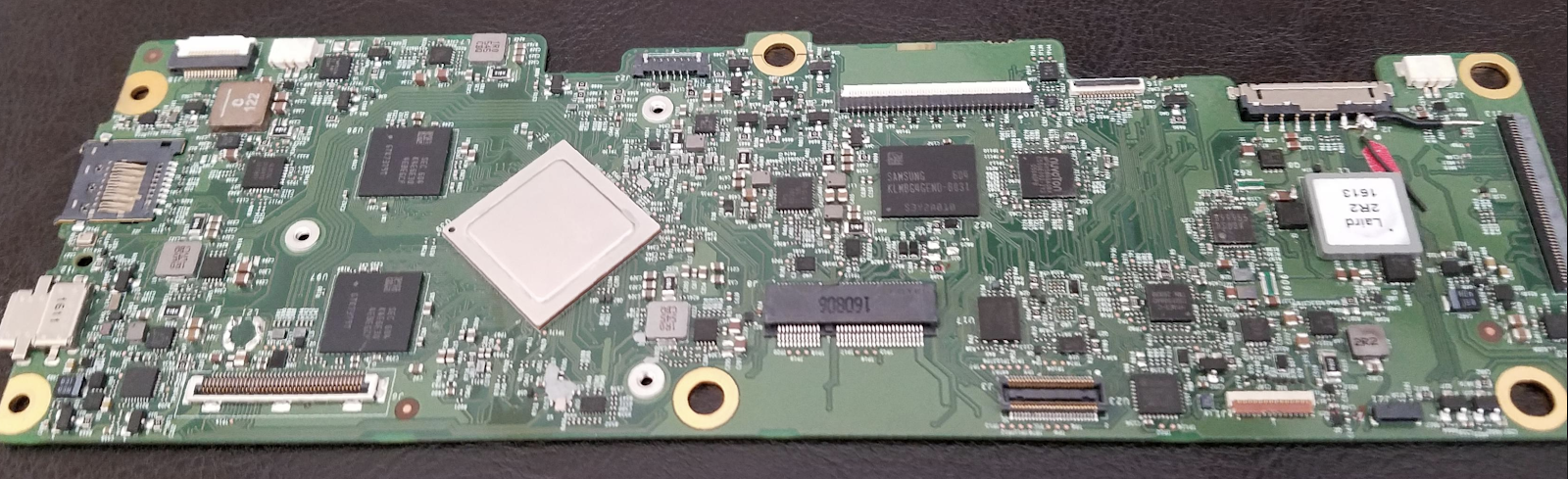
Image credit: Author - The P1 version of a motherboard for a laptop/tablet chromebook
Great systems start with solid documentation, strong communication, and trust that everyone is going to hit their mark. The first iteration is to see if things work. The second is to see if it fits and the third has to have 100% of both of those things. In the words of the cold warriors of ancient times, “Trust but verify.” Multiboard systems are expected to be complicated by their nature. The different voltages have to be over- and under-powered in different combinations and over varying temperatures and so on. With all that is expected of these costly systems, it is incumbent upon the designer to take care that the system level connections are fully vetted before the die is cast