The Road to Becoming a PCB Designer
Everyone has to start somewhere. Building a foundation for success takes time and effort. If you don’t already have a mentor, you should find one. If you can’t find one, then use the internet. A vast array of thought leaders create video or written content and share their knowledge freely. It may not be obvious where to look but there are a few ways to get into the game.. Some people start out as Librarians or Drafters and wind up filling a void when the in-house PCB Designer or outside Consultant is not available. Finding your first CAD seat takes work - or luck; maybe both.
Think about the first book you ever read. It probably wasn’t Homer's The Iliad. Ponder the first meal you cooked. It wasn’t a souffle but you made it yourself and moved on to bigger and better things. Your first PCB Design isn’t likely to end up in the Guggenheim Museum of Modern Art in Bilbao. Just like that autumn morning when you were sounding out those monosyllabic words or putting bread into the toaster, PCB design will take a few tries before you are doing routers for Cisco. You never get to stop learning. I like to fall asleep watching YouTube videos of Professor David Anderson giving Physics lessons from behind a glass wall.

Image Credit: Prof. Dave Anderson UCSD
Printed circuit boards come in several flavors. The most common type is probably a two or four layer board that covers a few square inches. With today’s electronics, that’s actually quite a bit of space to fill. A junior designer may be called on to perform layout of adapters, interposers, extender cards and other basic layouts. There could be connectors and passive components but not necessarily any integrated circuits. If you find yourself doing the same board over and over again, it may be time to look for something else.
My first PCB designs had only one layer. The bottom side was an unbroken copper ground plane that was bonded to an aluminum “pallet”. The boards were fabricated and assembled in-house. Our design tool was AutoCAD. If a trace needed to cross another trace, we added a zero Ohm resistor or even a piece of wire. One of my coworkers at Microsoft came out of the same startup so, you see, it’s a small world after all. I digress.
Image Credit: DMR Electronics - Similar to my first boards; note the lack of silkscreen. We didn’t even have soldermask.
The schematic was a single page; usually with one device nested in a slot. The artwork was created with a pen-plotter that used a cutting tool rather than a pen. The plotter scored the semi-transparent sticker known as rubbylyth and we peeled up the parts that were to become the air gaps. This was one step up from producing artwork manually. Be glad that we live in a better world now.
An education can be had on the job if you land somewhere that does electronic assembly. A broken phone or other electronic device will showcase the techniques that a designer used. When I see something like that along the side of the road, I’m tempted to check it out. Curiosity, creativity and a vivid imagination are a good place to start.
The first-time designer will benefit from a solid understanding of the following 10 things:
-
Education: Not only electronics but also basic physics and mathematics including geometry. Good communication skills are a must. There’s a bit of showmanship involved with managing expectations. A degree wasn’t always required. I managed to open some doors after six months in a trade school. Those high-school drop-out opportunities have faded away over time.
-
The pioneers: Names like Faraday, Henry, Ampere, Volta, Joule, Coulomb, Gauss and Ohm may be familiar. Also take the time to look up Gustav Kirchoff who built on Georg Ohm’s work. That leads to Maxwell’s equations and unlocks the foundation of electronics.
-
Getting the Job: Interviews can be tough. Preparation helps. To prepare for an interview with the Chromebook team at Google, I watched hours of videos about laptop repair. After a phone screen and a full day of on-site interviews, they still had more than one candidate. I was called in for a final exam with a duo of Managers. After the three rounds, they made me an offer that I couldn’t refuse.
-
The Kick-off: Somebody needs a board and you got the job. Expect a data dump and be ready to provide a time estimate. It seems prudent to sand-bag in case something goes awry. That’s a non-starter. They want a best-case scenario that you will adjust as you go. Set a few milestones to stay on course. If you want to stick around, you’ll execute the plan.
-
The Library: Any new components need to be accounted for. If your company has a librarian, you might be waiting for some footprints. Don’t let that prevent you from getting to the critical parts of the design. If you’re doing your own, make the most of it. A lot of the lingo is baked into the data sheets beyond the footprint diagram.
-
Place and Route: This is the main design work that starts with a board outline and a netlist that pulls in the library and the logic. Floorplanning is the first step. Determining the ideal stack-up is a close second. More often than not, these attributes will go through some iterations along the way.
-
Design Rule Checking: With any luck, there will be a set of constraints that capture the nominal geometry of the power domain and any electrical properties associated with various connections. Trace width, length and spacing are the first concerns but there are many subtleties involved as the design complexity increases.
-
Drafting: Notes, dimensions and details like hole charts and stack-up diagrams are an integral part of every document package. This is in addition to the actual artwork layers. Metal layers, soldermask and ink layers make up the bulk of the artwork. Data that is not part of the board that you’re also responsible for include a stencil for the solder paste deposition and a file that drives the pick and place machine.
-
The Design Review: Be ready to explain any decisions you made in getting to the optimum layout. It is rarely difficult to work with one person. The vast majority mean well. Mix in an Analog and a Digital type and you can be in the middle of a tug-of-war. Larger outfits will have an expert for everything.You get a chance to hone your cat-herding skills.
-
Tape-out: Compiling all of the data in a format that is suitable for fabrication and assembly. A good bet is that everything changes except the tape-out date. Archives are often broken out between fabrication and assembly. If you ended in a rush which is quite likely, go through and eyeball everything once more.
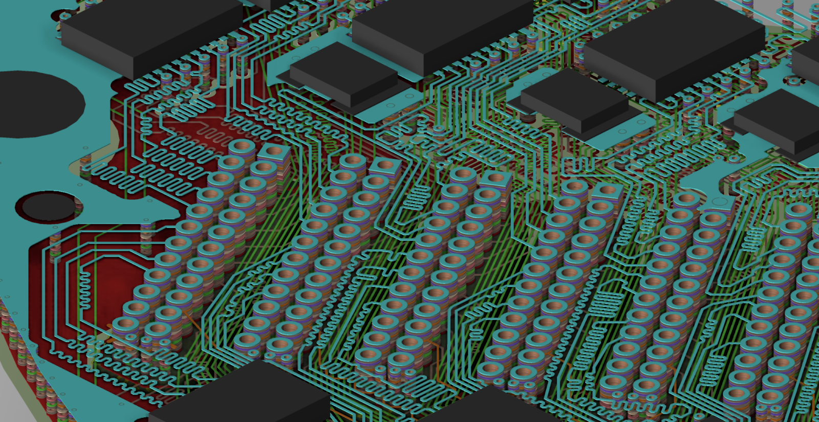
Image Credit: Author - An isometric view helps with a different perspective.
And that’s the short version. If any of the terms or themes are unclear, you’ll have to bootstrap your way to proficiency. Printed circuit board design can be frustrating. It can be boring. It can be challenging. It can be rewarding. It can be whatever you make of it. Make something of it.