High Speed Design and Analysis


Gain insight on designing reliable high-speed PCBs, from impedance control and differential pair routing, through HDI implementation, RF considerations, and timing analysis.
Sample content thumbnail
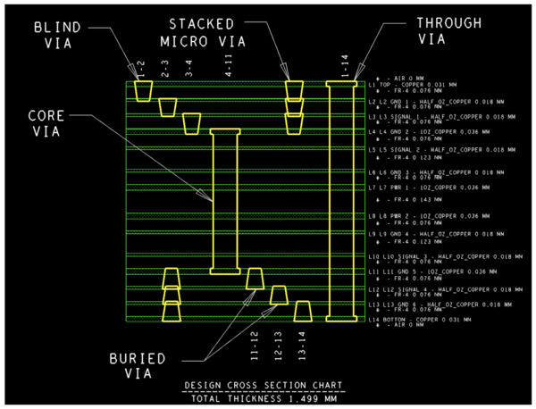
An Introduction to Microvias in PCB Design
Learn how microvias improve PCB design by enhancing signal integrity, power integrity, and thermal management in high-density interconnect (HDI) technology.
View Now
Sample content thumbnail
Navigating Signal Integrity Challenges in High-Speed PCB Design: Practical Tips to Solve Common Obstacles
Tackle signal integrity issues in PCB design with expert tips on SI challenges like impedance & ground planes using Cadence tools.
View Now
Sample content thumbnail
Grounding and Return Paths: Advanced Techniques - Part Two
Explore grounding techniques in high-speed PCB design to ensure signal integrity, reduce EMI, and optimize DDR, USB, PCIe, and RF system performance through smart design strategies.
View Now
Sample content thumbnail
Grounding and Return Paths: Essential for High-Speed Designs - Part 1
Discover how grounding strategies impact signal integrity, EMI/EMC, and power delivery in high-speed PCB design. Avoid failure with expert-backed tips.
View Now
Sample content thumbnail
Differential Pairs: From Basic Concepts to Advanced PCB Routing
Differential pair routing is at the heart of high-speed PCB design. This blog summarizes practical layout strategies for USB, HDMI, DisplayPort, PCIe, and Ethernet, covering impedance control, length
View Now
Sample content thumbnail
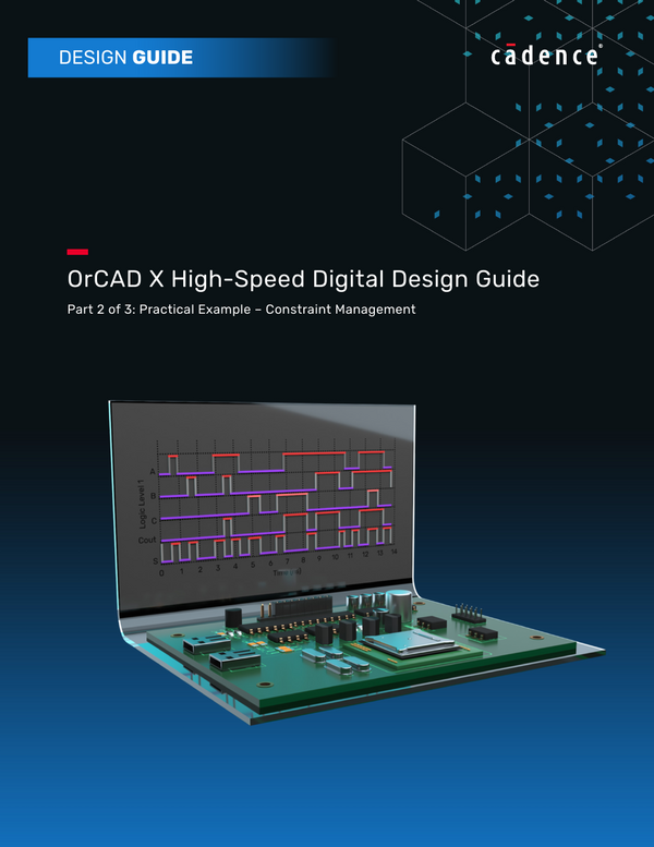
OrCAD X High-Speed Digital Design Guide Part 2
Part 2 of 3: Understanding High-Speed Digital Design Problems
View Now
6 results found
Evaluate how our PCB software fits in your design workflow.