Backdrilling in PCB Manufacturing
Backdrilling in PCB Manufacturing
Plated through holes (PTH) are great. They electrically connect two or more layers together, and serve as convenient connecting points for traces and components throughout a multilayer PCB. PTHs are mechanically sound, and can also be used as mounting holes.
But there’s a dark side to PTHs. Often times you don’t need the via to run the entire thickness of a board. The unused portion of the PTH that serves no functional purpose to the circuit is called a stub. And in high signal circuits, it can become significant source of signal distortion.
If your PCB is suffering from deterministic jitter, a high bit error rate (BER), signal attenuation, and other EMI problems, backdrilling may be the solution you’re looking for. In this post, we’re going to cover backdrilling, a handy technique for removing problematic stubs from PTHs.
What is backdrilling?
Back drilling (a.k.a controlled depth drilling or CDD) involves using a drill bit slightly larger in diameter than the PTH to remove the conductive plating or stub from the hole. In practice this is achieved by re-drilling the PTH down to a predetermined stub length less than 10 mils from the signal layer.
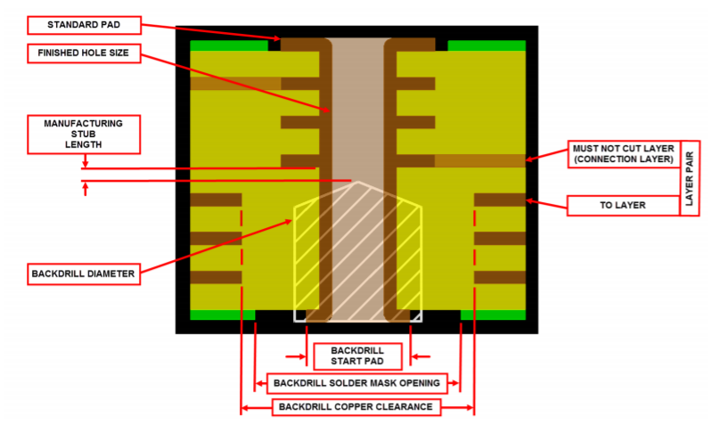
If the functional portion of the PTH is connecting two internal layers, it may be necessary to remove the stub from both the top and bottom of the board.
How via stubs generate noise
There are a number of problems that can be traced back to unused via stubs in high signal circuits. Let’s take a closer look at some of the issues caused by stubs:
-
Deterministic Jitter: Clocks are all about timing, and the degree to which that timing is off is called jitter. If the timing distortion is periodic (i.e. bounded), it’s called deterministic jitter.
-
Signal attenuation: When you attenuate a wave, its amplitude decreases resulting in a weaker signal.
-
EMI radiation: It’s possible for a via stub to behave as an antenna, radiating EMI.
So how exactly do via stubs cause jitter, attenuation, and EMI in high signal circuits?
When a signal travels down the length of a PTH it splits at the junction between the internal trace and stub. The signal that travels down the length of the stub gets reflected before returning to the trace junction where it again splits with some of the signal returning to source and the other following the trace.
In this manner it’s possible for the timing in a reflected wave to be so off its troughs actually cancel out the peaks (or vice versa) of an incoming signal. It’s easy to see how while this might not be a problem at lower bit rates, the increase in signal speed increases the noise generated from the split path created by the via stub. In other words, jitter leads to attenuation, higher BERs, and, in the presence of other electrical fields, EMI radiation.
How Cadence PCB tools can help you plan for backdrilling
There’s a bit more to backdrilling than just taking a slightly larger drill bit to the back of your PTHs. You’ll want to perform some electrical analysis to identify problematic stubs, and follow up with a plan of action to not only remove as much of the offending stub as possible, but also meet copper clearances to avoid damage.
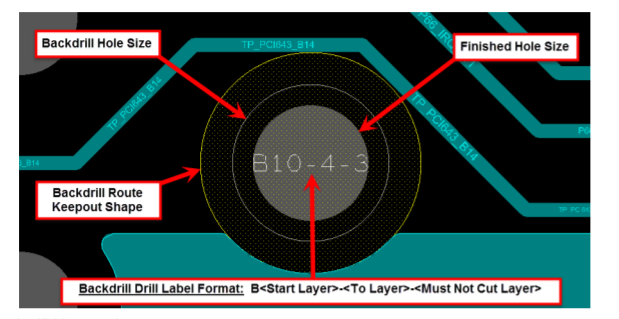
Cadence PCB you all the tools you need to factor backdrilling into your designs. It lets you create a padstack that contains information such as the minimum stub length and necessary clearances. With the padstack you can clearly identify special drill labels such as a hollow circle showing the backdrill diameter, as well as route keepouts automatically generated based on the clearances you specified in your padstack:
If you’ve noticed attenuation, jitter, and other noise issues in your design, unused via stubs could be the culprit. Ready to reduce noise in your designs with backdrilling? Check out Cadence PCB today!