Addressing Electromigration and IR Drop Within VLSI Interconnect Downscaling
Key Takeaways
-
Electromigration has an effect on IR Drop
-
Electromigration also has additional effects on circuit designs to consider
-
You can design interconnects more intelligently to combat adverse effects
Just imagine contacting your dear ones only on and off. You’ll miss out on a lot of things, right? The same applies to VLSI technology. Any minor miscommunication or time delays between chip circuit blocks can even make the system functioning at risk.
Interconnects are local, intermediate, and global communication lines in VLSI circuits, and their design and physical state are significant for achieving IC reliability. Interconnects are commonly made of metal wires and they are exposed to electric fields as they carry current. Electromigration (EM) and IR drop are two unavoidable casualties that make the interconnects susceptible to degradation.
When subjected to high current density, congested interconnect transports metal ions in the direction of electron propagation. This process of electromigration (EM) erodes and accumulates interconnect metal forming holes and spurs respectively. The lower geometry of interconnect and the influence of EM enhances the resistance and thereby IR drop issues. The EM and IR drop in interconnects are accountable for reliability issues and reduced lifespan in deep submicron VLSI circuits. In upcoming sections, let’s discuss some EM driven issues on interconnects and their design solutions.
IR Drop Intensifies in the Presence of EM
With the decrease in the device dimensions, there is speed and current density shoot up in VLSI systems. The vulnerability of power and clock signal interconnects to EM is more in high-density IC packages. Under the effect of EM, interconnect narrows down in the downstream whereas interconnect and via in the upstream gets metal deposition.
These makes and breaks caused by EM alter the resistance of interconnects and vias. The increase in the current traffic through the power interconnect worsens the IR drop and affects the device performance. The frequent switching activity intensifies the IR drop in clock interconnect and slows down the device speed. If your IC design includes multi-interconnect structures with different widths, you’ll slightly succeed in the IR drop mitigation. Your improved interconnect design can reduce the signal time delay between the VLSI circuit blocks and also minimize the clock skew.
Other After-effects of EM and Their Design Solutions
Will you keep calm if you get an official document in a jumbled format? Likewise, any crosstalk or error in the signal propagation irritates the proper functioning of VLSI circuits. The EM effect starts with intermittent glitches in the circuit logic and subsequently results in device instability. Some of the after-effects of EM are:
-
Interconnect delays: The rise in capacitance and resistance of the interconnect extends RC time delay in the signal propagation. The interconnect delay limits the IC speed and its performance characteristics. If power dissipation is not your concern, try inserting interconnect repeaters to reduce time delay.
-
Via open defects: As the metal decays in vias, two types of defects are created:
-
Resistive-open (ROP) defect which is similar to a defective resistor connected between two interconnects that should be connected.
-
Stuck-open (SOP) defect which is an open circuit between two interconnects that should be connected.
-
The substitution of single-cut vias by multi-cut vias provides back-up paths during ROP and SOP defects. The parallel connection of vias also helps to reduce the effective resistance of the interconnects.
-
Poor noise immunity: The uneven surfaces, stray impedances, impedance mismatch, and proximity of adjacent interconnects are some triggering factors affecting the chip signal integrity. The occurrence of false logic states, lowered noise margins, and reduced clock speed can be improved by shielding the interconnects.
-
Reduced lifetime: In deep submicron VLSI technologies, the depreciation in the interconnect quality plays a key role in reducing the EM lifetime. The void dimensions and time to develop a deadly void are derated under EM effect and thus interconnect mortality rate goes high. The following IC design modifications can improve the EM lifetime.
-
Widening the interconnect width: which is not practical with downscaling and nanoscale IC technology.
-
Replace Aluminium (Al) interconnects with Copper (Cu): Cu possesses lower resistivity, high electrical conductivity, and high melting point. According to Black’s equation, the Mean Time To Failure (MTTF) depends on activation energy, current density, and temperature. Table.1 gives the comparison of Al and Cu over some physical parameters and proves Cu interconnects to be better.
Table.1: Comparison of the physical parameters of Cu and Al estimated at the melting point
-
Use alloys of Al and Cu: The MTTF is high with the use of Al-Cu alloy interconnects. It also prevents interconnect junction spiking to some extent.
-
Avoid right angle bend in interconnects: as the curved bends are experimentally proved to achieve long chip lifetime and withstand EM stress.
-
Interlayer dielectrics: The adhesion between the metal interconnects and low-k dielectric material reduces the propagation delay and both inter and intra-capacitance in the substrate metal layers.
-
Interconnect dopants: The metals such as gold, silver, and manganese are introduced as dopants in interconnect metals. It improves the EM characteristics such as EM stress, resistance, and adhesion and ultimately the EM life expectancy of the VLSI circuits.
Easy Method of Designing Interconnects
The short-term reliability is an unacceptable trait in the complex nanoscale VLSI technology. The mainstream chip manufacturing industry overlooks a balance between the over-design and under-design of back-end-of-line (BEOL) elements, especially interconnects. This booby trap challenges the IC design engineer to come up with a state-of-the-art design that offers both high performance and phenomenal reliability within smaller footprint areas. You need to do several design iterations before finalizing the worst-case interconnect design with constraints such as area, current density, temperature, EM, and IR drop limits. Do you like to take this exhaustive path when there is an easy way out?
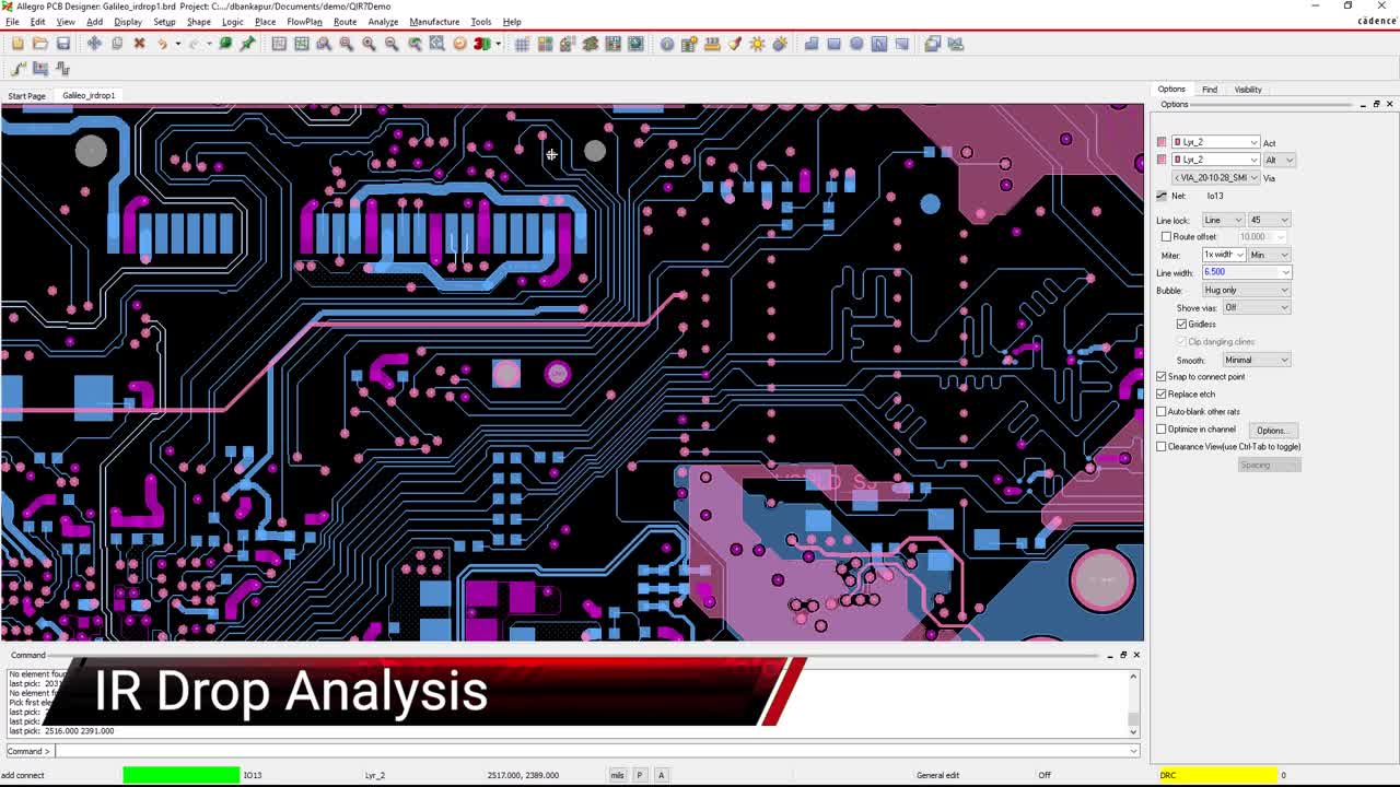
You can immortalize the interconnect design by using IC design and analysis tools. The cutting edge features in these computer-aided design tools can precisely guide your high-speed, high-density IC design in the right direction. You can access EM and IR drop analysis features of these design engines to identify the wear-out failures in interconnects without much difficulty. You can detect the hotspots violating EM and IR margins by interpreting the data available from this simulation platform.
Your interconnect design legalized through an IC design tool can bridge the gap between the market foot-print demands and design constraints. You’ll have to give yourself a chance to verify the interconnect design using IC design and simulation tools. For sure you’ll be blessed with a checkmate moment over the IC reliability issues.
If you’re looking to learn more about how Cadence has the solution for you, talk to us and our team of experts.