Top PCB Layout Recommendations for BGA Packages
Key Takeaways
-
Examine BGA packages in greater detail.
-
Explore PCB layout recommendations for BGA packages.
-
Learn to leverage the power of your PCB design tools for working with BGAs.
The 3D layout of a BGA footprint with internal trace routing beneath it.
As electronic devices continue to grow in their capabilities, they are also shrinking in size at the same time. Providing the necessary functionality for these smaller devices requires the latest advancements in component packaging technologies. Since their introduction in the late 1980s, one of the most popular component packages to fill this need has been the ball grid array (BGA).
Soon after their introduction, the BGA package began to make headlines as the next step in packaging technology. They offered higher interconnect density than both thru-hole PGA’s and surface-mount QFPs at comparable costs without the manufacturing problems associated with those packages.
Their popularity continued to escalate from there and they have become the default package for high-pin-count integrated circuits such as microprocessors and memory devices. Let’s take a deeper look into this and discuss some PCB layout recommendations for BGA packages.
A More Detailed Look at the Ball Grid Array Package
Ball grid array packages house the dies of complex integrated circuits without the pins or leads that are common with thru-hole or surface mount parts. Instead, they have pin pads spread out evenly on the bottom side of the package. Each of these pads has a tiny solder ball stuck to it with tacky flux, which will melt and form a solid joint during the solder reflow process of PCB assembly.
The BGA pin pads are spaced according to the size and number of pins for the device in pitches from 1.5mm down to 0.5mm. The solder balls themselves range in diameter from 0.75mm to 0.3mm.
As pin-counts increased on complex ICs, the standard surface-mount packages in use before BGAs became less desirable. These traditional packages with their pins on the perimeter had to increase in size in order to support the greater number of pins, which consumed a lot of room on the circuit board. And, as the size of the packages grew, they began to experience both electrical and manufacturability problems. With the switch to BGA packages, however, many of these problems were solved. A few specific problems that were solved were:
-
Size: Instead of relying on the perimeter of the part for the component leads, the pins of a BGA are spread out evenly underneath the package. This allows for smaller package sizes for the same number of pins compared to traditional dual in-line or quad-flat-pack parts.
-
Performance: With the pins spread out on the bottom of the BGA, the internal wires connecting the die to the pins are much shorter than they are in a DIP or QFP package. These shorter connections reduce their inductance and resistance, resulting in better performance for the part.
-
Thermal resistance: The shorter wires from the die to the pins in a BGA also reduce thermal resistance. This allows the heat generated by the part to dissipate more evenly to the circuit board, helping to cool the part.
-
Manufacturing: Without thru-hole pins or surface mount leads to bend, the handling issues of a BGA are much less than with other packages. The solder balls of a BGA are also self-centering during solder reflow which helps ease the manufacturing process.
-
Reliability: BGA packages solve the reliability problems of manufacturing high pin-count DIP and QFP devices. These packages, with their miniaturized pin widths and spacings, can easily form solder bridges between pins during assembly.
The use of BGA packages does pose some difficulties as well, however. For instance, with the BGA installed on the circuit board, visual inspection of the solder joints is virtually impossible without X-ray equipment or other advanced scanning tools. These problems can be overcome, though, and the benefits of using BGA packages far outweigh their faults.
Next, we will look at some considerations to keep in mind during the placement of BGA packages during PCB layout.
A BGA package placed on the top of a circuit board.
Component Placement PCB Layout Recommendations for BGA Packages
The more complex the BGA parts that you are working with, the more you will have to plan ahead in order to successfully route each pin to its associated net. High pin-count BGAs with their pins on a 0.5mm pitch will need careful planning to design escape routing patterns for all of their nets. This will take a lot of forethought in component placement long before you get into routing your traces.
As always, start your placement floorplanning with the fixed components such as connectors, switches, and other IO devices first. You will also want to keep the thermal considerations of the board in mind to ensure that your hot-running BGAs will have the airflow they need to stay cool. Processor and memory chips need to be close enough to their off-board connectors so that they don’t have to run long trace lengths throughout the board. At the same time, you must provide enough room for all of the parts of the signal path to cleanly fit without their traces having to wander too far to reach them.
As you begin your placement, remember to give your BGA parts enough room for all of their routing around them. These parts should have a lot of bypass capacitors associated with them, and they need to be placed directly next to the pins that they are connected to. Next, the components that are part of the signal paths need to be placed sequentially between the source and load of the signals. This may require altering large portions of your placement in order to fit these parts in, so be prepared for interactive work to finalize the placement.
Another thing to remember is that in addition to good signal integrity, you need to design for good power integrity. This means placing different power supplies close to the areas that they supply without allowing their circuitry to get mixed in with the sensitive digital circuitry of your BGAs.
With your parts placement arranged in the most optimum way, it is time to start routing the nets of the BGAs.
Selecting the vias to be used in PCB design CAD tools for routing in and around a BGA package.
Trace Routing Tips for Connecting BGA Packages
The first thing to do is to plan the escape routing or “fanouts” from the fine-pitch surface mount components like your BGA parts. Escape routing is much more than just drawing a short trace and dropping a via; it has to be planned together with the component placement, layer stackup, signal integrity needs, and routing density. For high pin-count fine pitch BGAs, additional board layers or high-density interconnect (HDI) routing tactics may be required. Before committing to this, however, it is always best to check first with your PCB manufacturer to confirm prices and their ability to build an HDI board.
When it comes to routing the escape traces and vias out of a BGA, start first with the outer rows. Using diagonal routing, these traces will be the simplest to lay down. From there, you can start working your way in through the rows of pins. For BGAs with larger pin pitches, a short trace segment can be used to connect to a via next to the pad in what is known as a “dog-bone pattern.”
Larger pin-pitch BGAs will also allow you to route between the pads as well. For smaller pitches, it may be necessary to use via in pads, although this will add to the manufacturing costs of the board. Again, check with your manufacturer first to confirm what level of PCB technology they will be able to build for you and at what price. Here are the vias that you will be working with:
-
Thru-hole: This is the most common via used in a circuit board. Created with a mechanical drill, they penetrate all the way through the board but do have minimum size restrictions. For a standard width circuit board, the minimum drill size is usually no less than 6 mils.
-
Blind and buried: These vias are also created with a mechanical drill, but will either penetrate only partially through the board or start and stop on internal layers of the board. Blind vias can be embedded in BGA pads, and both blind and buried vias require drilling the layer pairs of the board before they are laminated together during PCB fabrication. These extra steps make blind and buried vias more expensive to manufacture, but the increase in cost may be the necessary choice on dense boards.
-
Micro: Created with a laser, these vias are smaller than what can be drilled mechanically, but they usually span only two layers due to their smaller size. Microvias can be stacked together or staggered side-by-side to achieve the required results. Although they do cost more than a mechanically drilled via, their ability to be embedded seamlessly in a BGA pad makes them ideal for fine-pitch part fanouts.
As you route your escape patterns out of a BGA device, remember that higher pin-count parts will require additional board layers. All of the vias needed to route out from the pins will take up the routing channels that you need for the traces. You may find yourself having to add another board layer for every two rows of pins on the BGA.
One thing that you can do to help yourself is to consult the recommended routing patterns that many part manufacturers will include in their component’s datasheet. You should also set up the design rules and constraints in your PCB design tools to control the size of the trace widths and spacing for your BGA routing. We’ll take a look at that next.
The Constraint Manager in Cadence’s Allegro PCB Editor showing the vias assigned to nets.
Managing BGA Design Rules in PCB Design CAD Tools
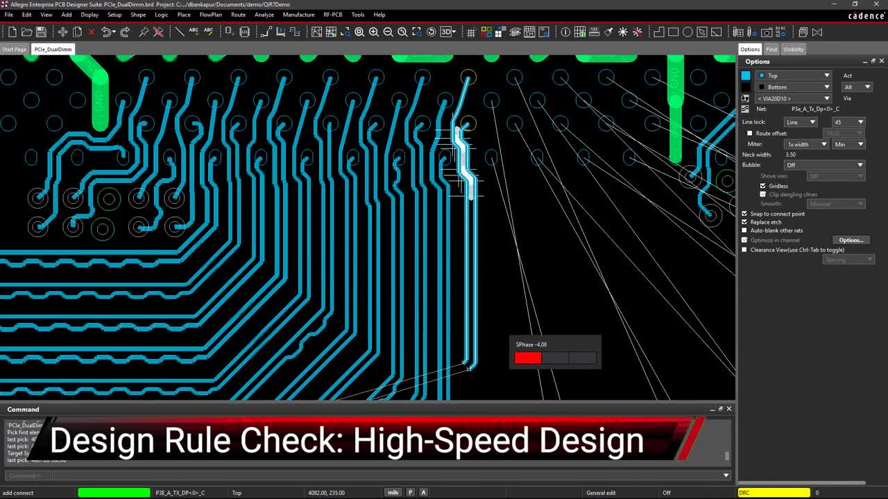
The high-speed designs that will require parts in BGA packages will usually have specific high-speed constraints associated with them. This will include specific nets that can only be routed on certain layers, differential pairs that have to be routed together, and different-sized traces depending on what nets are being routed. While a designer can easily keep track of a few of these rules, the hundreds of different nets and requirements associated with routing a BGA can be completely overwhelming. Here is where the help of a constraint management system like what is found in Cadence’s Allegro PCB Editor can be very helpful.
The Constraint manager that you see pictured above shows the vias assigned to the different nets on this board. Not only can you assign different vias to nets and net classes, but you can control the trace width and spacing values as well. This will enable you to easily route in and out of dense BGA areas without having to manually reset your trace widths and spacing each time you do. There are many other tips and tricks that can help you with trace routing in and around BGAs, and you can read more about them in this E-book.
If you’re looking to learn more about how Cadence has the solution for you, talk to us and our team of experts.