High-Speed Analog Layout Techniques in PCB Design
Key Takeaways
-
Setting up your PCB for the best analog signal performance.
-
PCB place and routing techniques for analog layouts.
-
CAD tools that can help your PCB design efforts.
Analog inputs from all of these sources must be converted to their digital counterparts
More than anything else, the exodus of workers from a traditional office setting to working from home has shown just how much we truly live in a digital age. From shared online documents to video conferences, remote workers are leveraging as much as they can from the computers and networks at their disposal. However, just because we are all part of this digital age does not mean we live in a digital world.
Our world is filled with sights and sounds that must be detected and captured by analog electronics. These analog signals must then be converted into a digital format to be processed by computers and other digital devices before being shared electronically across different networks. The job of converting these formats belongs to mixed-signal circuitry in PCBs, and they have quite the job ahead of them with today’s electronic requirements. Here are some high-speed analog layout techniques that can help mixed-signal PCB designs be successful in their tasks.
Mixed-Signal PCB Design
From what we see and hear to temperatures and motion, the number of sensory events captured by different electronic devices has become incalculable. Each of these actions or events are captured as analog signals, which must then be converted for processing in digital systems like computers. The job of this conversion belongs to analog-to-digital converters that are used in mixed-signal circuit boards within these systems.
Analog signals will vary depending on the magnitude of their source. For instance, the amount of light or sound detected by a camera or microphone will alter the amplitude of the signal being captured. However, analog circuitry is dependent on a continuous voltage or current for its signals and relies on precise control during their transmission and reception to be correctly interpreted. In comparison, digital signals have just two values; on and off. This structure allows for a larger margin of error in how they are transmitted, making their design easier than their analog counterparts.
A PCB designer must exercise the proper separation of analog and digital circuitry during layout to keep both of these signal types from affecting each other. We’ll look into different methods for doing this as we continue.
Analog layouts need a tight component placement
Component Placement and Trace Routing for High-Speed Analog Layout Techniques
Much of the ultimate success of your analog and digital circuits will rely on how well the layer stackup in your PCB design is configured. High-speed signals require a reference plane on an adjacent layer for a signal return path to minimize noise and improve signal integrity. Therefore, the configuration of the board layer stackup needs to be done with the general placement in mind to ensure adequate space for routing on the appropriate layers. Designers can accomplish this by relying on high-speed analog layout techniques like grouping components together by their function and blocks of circuitry to create a floorplan that will serve as a template for actual component placement. This floorplan needs to isolate digital and analog circuitry from each other in functional partitions, while interconnections between groups are arranged for the most direct routing.
With the floorplan complete, designers can move directly into component placement. Remember that the goal is to keep the routing as short and as direct as possible, so the parts must be configured in their placement accordingly. Here are some high-speed analog layout techniques and placement reminders to keep in mind when working with analog circuitry:
- Place parts for the most direct routing between each other.
- Do not place parts where you will be forced to route digital signals through analog circuitry and vice-versa.
- Keep your component placement as tight as possible to reduce the length of analog traces.
- Remember to place parts according to the design for manufacturability (DFM) standards recommended by your assembler.
- Keep noisier parts, like ADCs, away from the edges of the board and more centrally located.
Placing components and then routing is a workflow that many PCB designers use; however, it is sometimes helpful with analog layout to place and route simultaneously. Either way, here are some recommendations for analog trace routing:
- Keep the trace routing as short and as direct as possible. This routing should already be facilitated by the tight component placement that you’ve done and will help reduce the chances of impedance mismatches and signal reflections.
- Use wider trace widths when routing analog circuitry.
- Keep analog traces confined to a single board layer as much as possible. Vias can create inductance, and the less you have to transition between layers with vias, the better.
- Do not route analog traces through areas of digital circuitry or digital traces through analog areas.
- Keep analog and digital routing confined to their areas of circuitry as much as possible. This will further reduce the chance of mixed-signal crosstalk.
One final rule of routing both analog and digital signals is to never cross blocked areas of the reference plane with your traces. Routing through these areas on the reference plane can create noise due to a poor signal return path.
Routing a trace on an adjacent layer through this area could result in a blocked signal return path
Power Delivery Network Recommendations for Analog Layout
Both the analog and digital components of your design will need clean power delivered to them, but high-speed PCBs are often plagued by many problems with their PDN, such as transient ringing. This is often dealt with by including plenty of decoupling capacitors in the design and providing high interplane capacitance by placing ground and voltage layers adjacent to each other in the stackup. Once again, how the board layer stackup is configured is crucial to the success of your mixed-signal design.
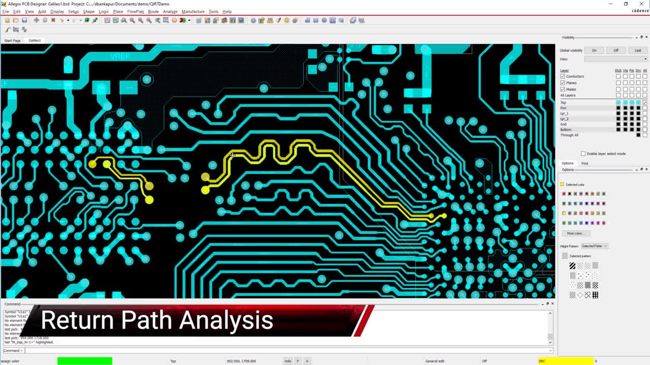
How you lay out the ground plane on your design is also essential to the board’s operation. As we mentioned earlier, signals should not be routed across areas where the ground plane is broken up. Whether it is gaps in the plane or areas of dense vias, as shown in the image above, the disruption of the ground plane could block the clear return path of the signal, forcing it to wander around on its way back to the source. This wandering is one of the major causes of EMI and reduced signal integrity in a design. To avoid these problems, ensure that your signals have a clear return path on the reference plane for the best board performance. Design tools, like Cadence’s Allegro PCB Editor, have advanced functionality to help design signal return paths, as demonstrated in the video at the top of this article.
One of the obstacles that can cause a big problem for signal return paths on a circuit board is a split ground plane. If your design includes a split plane, do not cross the split with your trace routing. The signal’s return path will be completely cut off, creating an even worse signal integrity problem. However, the better plan is not to split the ground plane at all. Although many believe that ground splits create better isolation between the analog and digital areas of circuitry, it can also create more problems than expected. We’ve already mentioned the issues with clear signal return paths, and there is also the chance of introducing common mode currents between the sections if a chassis ground is used. Instead, with a complete ground plane and the analog and digital areas of circuitry placed and routed separately, you will have clear return paths for those few signals that do have to travel between sections. Eliminating the ground plane splits can resolve many EMI problems and give you a cleaner design, as the analog and digital signals will naturally form tight return paths around their traces.
Obviously, many details need to be managed during PCB layout for a design like this. Working with an advanced design system can provide the next level of help to designers.
Cadence Allegro’s Constraint Manager being used to set up routing and via design rules
How to Use Your PCB CAD Tools
Placing components tightly to exacting space widths and routing differing trace widths and spacings for analog circuitry requires detailed database management. You will want to make sure to fully set up and use your CAD system’s design rules to control these constraints. In the picture above, you can see an example of the Constraint Management system in Allegro and how different values can be entered for component clearances, trace widths, and spacings for individual elements or classes of components and nets.
Cadence also helps designers with a wide assortment of circuit simulation and design analysis tools. Within Allegro, you also can view and check a PCB design in 3D to other circuit boards or mechanical objects within your complete system design. With tools like these, designers can handle more complex designs and complete them faster and with fewer errors.
To find out more about how a successful digital and analog design relies on high-speed analog layout techniques as well as a well-designed PDN, take a look at our E-book on the subject.
If you’re looking to learn more about how Cadence has the solution for you, talk to our team of experts.